
Datasheet

[AK4646]
MS0557-E-06 2011/06
- 65 -
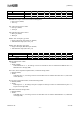
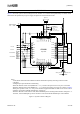
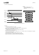
SYSTEM DESIGN
Figure 37 shows the system connection diagram for the AK4646. An evaluation board [AKD4646] is available which
demonstrates the optimum layout, power supply arrangements and measurement results.
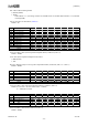
NC
ROUT
LOUT
MIN
RIN2
LIN2
LIN1
RIN1
NC
NC
SVSS
SVDD
S
PP
SPN
MCKO
MCKI
MPWR
VCOM
A
VSS
A
VDD
VCOC
NC
PDN
CSN
DVSS
DVDD
BICK
LRCK
SDTO
SDTI
CDTIO
CCLK
A
K4646
Top View
2
5
26
27
28
29
30
31
32
24
23
22
1
1
6
15
14
13
12
11
10
9
21
20
19
18
17
2
3
4
5
6
7
8
2.2k
2.2k
2.2k
2.2
k
External MIC
Internal MIC
0.1u
2.2u
0.1u
Rp
Power Supply
2.2 ∼ 3.6V
0.1u
0.1u
10
DSP
μ
P
Line Out
Speaker
Mono In
Cp
10u
Analog Ground
D
igital Ground
1u
1u
200
200
20k
20k
ZD2
ZD 1
Dynamic SPK
R1, R2: Short
ZD1, ZD2: Open
Piezo SPK
R1, R2: ≥10 Ω
ZD1, ZD2: Required
R1
R2
Notes:
- AVSS, DVSS and SVSS of the AK4646 should be distributed separately from the ground of external
controllers.
- All digital input pins should not be left floating.
- When the AK4646 is EXT mode (PMPLL bit = “0”), a resistor and capacitor of VCOC pin is not needed.
- When the AK4646 is PLL mode (PMPLL bit = “1”), a resistor and capacitor of VCOC pin is shown in
Table 4.
- When piezo speaker is used, 2.2
∼ 4.0V power should be supplied to SVDD and 10Ω or more series resistors
should be connected to both SPP and SPN pins, respectively.
- When the AK4646 is used at master mode, LRCK and BICK pins are floating before M/S bit is changed to “1”.
Therefore, around 100k
Ω pull-up resistor should be connected to LRCK and BICK pins of the AK4646.
Figure 37. System Connection Diagram