
Specifications
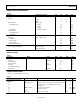

4 ADC with PLL,
192 kHz, 24-Bit ADC
Data Sheet
AD1974
Rev. D Document Feedback
Information furnished by Analog Devices is believed to be accurate and reliable. However, no
responsibility is assumed by Analog Devices for its use, nor for any infringements of patents or other
rights of third parties that may result from its use. Specifications subject to change without notice. No
license is granted by implication or otherwise under any patent or patent rights of Analog Devices.
Trademarks and registered trademarks are the property of their respective owners.
One Technology Way, P.O. Box 9106, Norwood, MA 02062-9106, U.S.A.
Tel: 781.329.4700 ©2007–2013 Analog Devices, Inc. All rights reserved.
Technical Support www.analog.com
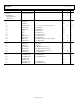
FEATURES
Phase-locked loop generated or direct master clock
Low EMI design
107 dB dynamic range and SNR
−94 dB THD + N
Single 3.3 V supply
Tolerance for 5 V logic inputs
Supports 24 bits and 8 kHz to 192 kHz sample rates
Differential ADC input
SPI®-controllable for flexibility
Software-controllable clickless mute
Software power-down
Right justified, left justified, I
2
S, and TDM modes
Master and slave modes up to 16-channel input/output
Available in a 48-lead LQFP
Qualified for automotive applications
APPLICATIONS
Automotive audio systems
Home Theater Systems
Set-top boxes
Digital audio effects processors
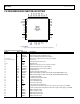
GENERAL DESCRIPTION
The AD1974 is a high performance, single-chip ADC that pro-
vides four analog-to-digital converters (ADCs) with differential
inputs using the Analog Devices, Inc. patented multibit sigma-
delta (Σ-Δ) architecture. An SPI port is included, allowing a
microcontroller to enable mutes and adjust many other
parameters. The AD1974 operates from 3.3 V digital and analog
supplies. The AD1974 is available in a single-ended output
48-lead L Q F P.
The AD1974 is designed for low EMI. This consideration is
apparent in both the system and circuit design architectures.
By using the on-board phase-locked loop (PLL) to derive the
master clock from the LR clock or from an external crystal,
the AD1974 eliminates the need for a separate high frequency
master clock and can also be used with a suppressed bit clock.
The ADCs are designed using the latest continuous time archi-
tectures from Analog Devices to further minimize EMI. By
using 3.3 V supplies, power consumption is minimized, further
reducing emissions.
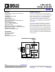
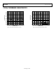
FUNCTIONAL BLOCK DIAGRAM
QUAD
DEC
FILTER
48kHz/
96kHz/192kHz
SERIAL DATA PORT
DIGITAL AUDIO
INPUT/OUTPUT
PRECISION
VOLTAGE
REFERENCE
12.48MHz
TIMING MANAGEMENT
AND CONTROL
(CLOCK AND PLL)
CONTROL PORT
SPI
CONTROL DATA
INPUT/OUTPUT
AD1974
ADC
ADC
ADC
ADC
ANALOG
AUDIO
INPUTS
SDATA
OUT
CLOCKS
06614-001
Figure 1.