ORDER NO. CPD0606050C1 Wireless Display CF-08TX1A1M This is the Service Manual for the following areas. M …for U.S.A. © 2006 Matsushita Electric Industrial Co., Ltd. All rights reserved.
1
2
Precautions Battery Pack Care should be exercised with regard to the following in order to avoid the possibility of overheating, fire or damage. Do Not Use With Any Other Equipment The battery pack is rechargeable and was intended for the specified equipment. Do not use it with any equipment other than the one for which it was designed. Avoid Heat Do not throw the battery pack into a fire or expose it to excessive heat.
Stop Using Should the battery emit an abnormal odor, become hot to the touch, become discolored, change shape, or become in any way different from normal, remove it from the wireless display and stop using it. NOTE The battery pack may become warm during recharging or normal use. This is completely normal. Recharging will not commence if internal temperature of the battery pack is outside of the allowable temperature range (0 °C to 45 °C {32°F to 122°F}).
CONTENTS 1. Specifications ··················································································································1-1 2. Introduction······················································································································2-1 3. Description of parts ·········································································································3-1 4.
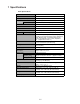
1 Specifications Main Specifications Model No. CF-08TX1A1M CPU Intel® PXA270 Processor 312 MHz Memory (ROM/RAM) 32 MB (Flash) /64 MB Display Method 10.4 XGA type Internal LCD Display 65,536 colors (1024 × 768 pixels) Wireless LAN Built-in Bluetooth Built-in LAN IEEE 802.3 10Base-T, IEEE 802.3u 100Base-TX Sound Card Slot WAVE playback, Monaural speaker SD Memory Card*1 × 1, Data transfer rate=4.8 MB per second*2 Interface USB Port × 1 (USB1.
Software *1 *2 *3 *4 *5 *6 *7 *8 Microsoft® Remote Desktop Connection, Citrix® ICA® Client, Microsoft® Internet Explorer 6.0 This slot does not support the MultiMedia card. Operation has been confirmed for Panasonic SD Memory Cards with up to 2 GB capacity. Theoretical value and not the actual speed. The transfer rate does not become higher even if you use a card that supports the higher transfer rate. The AC adaptor is compatible with power sources up to 240 V AC adaptor.
2 Introduction Copyright This manual is copyrighted by Matsushita Electric Industrial Co., Ltd. with all rights reserved. No part of this manual may be reproduced in any form without the prior written permission of Matsushita Electric Industrial Co., Ltd. No patent liability is assumed with respect to the use of the information contained herein. © 2006 Matsushita Electric Industrial Co., Ltd. All Rights Reserved. Disclaimer Wireless display specifications and manuals are subject to change without notice.
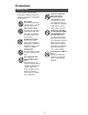
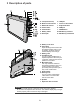
3 Description of parts A. LCD (Touchscreen) H. LAN port B. Wireless LAN antenna I. Cursor control button C. Bluetooth antenna J. Keyboard button D. Power status K. USB port E. Power button L. USER button F. Battery status M. SD Memory Card slot G. DC-IN jack N. SD Memory Card status A. Battery cover latch B. Hand strap Adjust the length of the belt so that the wireless display does not fall by mistake, and firmly hold the wireless display when using it. C. Battery pack D.
Using the Tether The tether can be attached to the upper right or upper left corner of the display. It prevents the pen (included) from falling accidentally.
4 Starting up/Shutting Down Starting Up 1 Turn on the wireless display. When you log on as a Supervisor When you log on as a User Press the power button with the USER button pressed. • If you do not do so, even when you set enter the Supervisor Password, the wireless display will run in the User operating environment. Press the power button. 2 When the [Enter Password] screen appears, enter the password, and then tap [OK].
C. Password A. Auto Launch To set the password B. Wait for Network Connection • If a User Password has been set in the • When the Supervisor does not [User] tab of [Security (Supervisor)] add the check mark for [Allow screen, User cannot delete a password. Change Auto Launch] in the • If a User Password has not been set in [User] tab of the [Security Setthe [User] tab of [Security (Supervisor)] tings (Supervisor)] screen, [Auto screen, User cannot create a new Launch] and [Wait for Network password.
When returning the wireless display to its condition at the time of shipment Perform the following procedure while the wireless display is turned off. A Connect your wireless display to a power outlet. B Press the power button with the keyboard button and USER button pressed until the message “Reset the device to factory default...” appears. When the [Enter Password] screen appears, enter the Supervisor Password and tap [OK]. C Select [Yes].
5 Diagnosis & Repair 5.1. Basic Procedures The basic procedures for diagnosis, disassembly, and test of defective parts of a set to be repaired are summarized below. For details, refer to relevant pages in the Service Manual. Flow Chart OCCURRENCE OF TROUBLE Insert the AC plug. Press the Power button, while pressing the USER button and the Cursor control button at the same time. Self Test Program Self Test Program start up.
5.2. Troubleshooting Please take note of the following two points with regard to troubleshooting: 1. Know-how of diagnosis upon occurrence of heavy troubles, e.g. ‘Set cannot be turned ON’, ‘Set fails to start’, ‘No display on screen’, etc. 2. Explanation of each trouble, mainly symptom of trouble in operation. Flow Chart START START Set cannot be supplied with current. Power lamp fails to light up. Pay attention to the following points when in pursuit of the cause of a troubleshooting. 1.
5.3. Self Test Program 1. Introduction This description explains Self-Test Program of this Test. 2. How to Start-up (1) Connect the AC adaptor. ( Unless you connect the AC adaptor, the Self-Test Program does not start. ) (2) Connect the AC adaptor. Press the USER button and Cursor Control button at the same time, then press the Power button to turn on the computer. Self-Test Program starts automatically. 3. Self-Test This test is to check if the device is disconnected. 3.1.
3.1.3. Test register check for the source microcomputer. Check the test register of the source microcomputer 3.1.4. ID check for 2700G Confirm the ID of 2700G. 3.1.5. Chip ID check for LAN9118 Check the test register and chip ID of LAN9118. 3.1.6. Card detection pin check and tuple information check for PCMCIA When you cannot obtain the tuple information, wait 0.5 second, then try to obtain the information by calling for API. Repeat this up to 10 times. (The maximum time required: 5 seconds.) 3.2.
If the results of all items are OK, the following display appears. *** SELF TEST *** CPU Type : OK SDRAM March Test : OK Embedded Controller : OK 2700G : OK LAN9118 : OK PCMCIA : OK Overall Result : OK If only the PCMCIA result is NG, the following display appears. *** SELF TEST *** CPU Type : OK SDRAM March Test : OK Embedded Controller : OK 2700G : OK LAN9118 : OK PCMCIA : NG Overall Result : NG After the test result is shown on the display, the program hangs. 4.
6 Troubleshooting Follow the instructions below when a problem has occurred. For a software problem, refer to the software’s instruction manual. If the problem persists, contact your technical support office. Starting Up Cannot start up. The power indicator or battery indicator is not lit. Connect the AC adaptor. Insert a fully charged battery. Remove the battery pack and the AC adaptor, then connect them again. Cannot turn on the wireless display.
Shut Down Cannot shut down. Press the power button for four seconds or longer to shut down the wireless display. Sound No sound. Confirm the volume for [Quick Menu] or [Volume & Sounds] in Control Panel. Unable to hear sound in stereo. Playback conditions vary depending on the server. • If you are connecting through Microsoft® Remote Desktop Connection or a web server, you will hear monaural sound even if the original sound is stereo.
7-1 Battery CN PMC Battery Monitor M16C28 PWM FL BackLight Touch Screen on LCD Panel AC97 Codec with Touch screen controller WM9712 (Wolfson) Mic/Amp/Speaker Power-MG I2C I/F SD/MMC/SDIO AC97 I/F Crystal 13.000MHz 32.786KHz Codec MC145483 Motorola POWER MAX1586 DC-DC Crystal 24.576MHz CF-08 Block Diagram USB Host1 Cradle I/F USB Host2 I/O 1.8V 13MHz-312MHz,Core 0.85-1.
7-2 5200mAh 7.4V SYS_EN DC/DC (LTC3406) Voltage Regulator 2.5V R FET OVP# FET 2700G Power V2700_LM(1.8V/2.5V) V2700_PLL(2.5V) FET Charger (LTC4008) FET V2700_Core(1.2V) Voltage Detector & OVP# PMC Battery Monitor M16C28 ACIN Voltage Regulator 1.2V NTC Battery VCC_3P3V VCC_MEM(1.8V) VCC_IO(3.3V) VCC_MEM(1.8V) (16V/2.5A) Cradle Con (16V/2.5A) AC Adapter VCC_BATT(3.3V) R PWR_EN FET FET FET VLAN(3.3V) WLVCC(3.3V) Voltage Detector FET Voltage Regulator 3.
8 Wiring Connection Diagram SW LED PCB CN501 SW500 CN500 SW502 SW501 USB PCB LCD CN400 CN401 USB Microphone IO POWER PCB Headphone INVERTER CN6 CN7 CN302 DC-IN CN301 CN300 BATTERY PACK AUDIO CON PCB CN4 LAN CN9 CN12 CN7 MAIN PCB CN13 SD CARD SLOT CN3 CN9 CN4 CN10 CN6 CN1 CN2 CN8 WLAN PCB DOCK CON PCB CN1 CN600 SPEAKER CN601 CN602 EXPANSION BUS ANTENNA PCB R Connector by Cable Direct connection by Connectors CN2 CN3 ANTENNA PCB L Parts on Bottom Side 8-1
9 Disassembly/Reassembly Note: Power off the computer. Do not shut down to the Suspend or hibernation mode. Do not add peripherals while the computer is in the Suspend or hibernation mode; abnormal operation may result. 9.1. 9.1.1. Disassembly Instructions Preparation 5. Pull the tab of the Battery Pack and remove it from the wireless display. Be sure to make the following preparations before disassembling. • Shut down Windows and turn off the power. • Disconnect the AC adaptor.
9.1.4. 3. Remove the 12 Screws . Lamp Cable Spring Removing the Main PCB Rear Cabinet Cable Holder Sheet Connector(CN6) Connector(CN7) Connector(CN3) Connector(CN13) Connector(CN4) Connector(CN9) Main P.C.B. Connector(CN12) Connector(CN10) Cable Inverter IO Power P.C.B. 1. Disconnect the seven Cables from the Connectors (CN3,CN4,CN7,CN9,CN10,CN12,CN13). 2. Remove the four Screws . 3. Remove the Main PCB. 4.
9.1.6. Removing the WLAN PCB 9.1.8. Removing the Speaker Antenna Cable Speaker Hold Sheet Speaker B Antenna Cable WLAN P.C.B. Lamp Cable Spring A B A 1. 2. 3. 4. 1. Remove the two Screws . 2. Remove the Speaker Hold Sheet. 3. Remove the Speaker fixed with the two-sided tape. Remove the two Antenna Cables. Remove the four Screws . Remove the Lamp Cable Spring. Remove the WLAN PCB. Screws :XSB2+4FNL 9.1.9.
9.1.10. Removing the WLAN L PCB (CN600,CN601). Insulation Sheet Dock Con P.C.B. Docking P.C.B. Sheet Base Joint Cover Antenna Cable WLAN L P.C.B. 3. Remove the five screws . 4. Remove the Base Joint Cover, the Docking PCB Sheet and the Dock Con PCB. 1. Remove the Insulation Sheet. 2. Remove the Screw . 3. Remove both the Antenna Cable and the WLAN L PCB. Screws :DXQT26+D5FNL Screw :DFHE5025XA 9.1.11. 9.1.13.
9.1.14. Removing the LCD Unit and the Inverter Pet Tape Inverter Case Inverter Inverter Connector LCD Unit 1. Disconnect the Cable from the Inverter Connector. 2. Remove the Inverter with the Inverter Case. 3. Remove the Pet Tape. TS Noise Tape LCD Unit Cable Clamper 4. Remove the TS Noise Tape. 5. Remove the Cable from the Clamper. 6. Remove the LCD Unit.
9.2. 9.2.1. Reassembly Instructions Attention when CF-08 series is repaired • Please execute writing BIOS ID when you exchange the Main Board. • Parts (Sheet and rubber) etc. related various the Conductive Cloth and Heat Spreader cannot be recycled. Use new parts. 9.2.2. Setting the LCD Unit and the Inverter 1. Attach the LCD Unit. 2. Attach the TS Noise Tape. 3. Put the Cable into the Clamper. TS Noise Tape LCD Unit Cable Clamper 4. Attach the Pet Tape. 5.
■ Preparations for backlight For appearance standard information of the LCD process, refer to the "Common Assembly Instruction Manual". LCD Prism Sheet Remove the protection films. (both sides) Holder Sheet LCD 0~0.5mm Prism Sheet wide side Handle with care. (Avoid fingerprints or scores.) 1 Holder Sheet Attach two sheets. Details of "A" Insert into the inside the ribs. (4 places in total) 0~0.5mm Avoid running over the wall. narrow side 0~0.
Holder Sheet Positional Relation Chart for 1 and 2 Holder Sheet LCD Refrection 0~0.5mm Sheet LCD Refrection Sheet Insert after attaching 1. Make the silver side inside. Insert into the inside the ribs. (4 places in total) To avoid deflection, do not attach 2 too close to the Frame. LCD Refrection Sheet LCD FRAME Avoid running over the rib. (both sides) (Running over causes moire.) Insert into the inside the Hooks.
LCD PWB Sheet Parts for electricity removing work Refrect Tape Press the Sheet along the edge of the Reflector (Avoid floating.). 0~0.5mm Attach here. Lengthwise: Match to the top end of the Reflector. Crosswise: Match to the rib of the Frame. Bend to the lateral side. Standard attaching position of 1 Match to the PWC outline. Pet Tape 1 CN Run over the end of the CN metal (0.5 to 1 mm) Match to the Kapton side and attach to the Reflector side.
■ Preparations for Touchscreen Front Case Assy TS Tape Attachment Standard Attachment Standard Attachment Standard ■ Assembly of the Touchscreen A TOUCH SCREEN ASSY Protect *Remove it parallel to the T/S. Sheet OK stiffening plate side Laminate Film 25–1mm Attach to the center of the display surface. (Using the jig) T/S NG Details of "A" Laminate Film TS FPC Spacer Dimensional tolerance: +0.2 0~0.5mm T/S (Note) Apply the load 20 to 30N (2.0 to 3.0 Kgf) to the Cushions.
■ Assembly of the LCD Block 0~1mm Safety Working Attach the Conductive Cloth to the Mg side. (Remove the Release Paper only of the attaching part.) Pet Tape 1 When the Cable is close to the edge (more than 4 mm than the standard position), ensure that the Cable is not wound in other parts. Pet Tape 1 LCD Block Pet Tape 1 edge standard: +0.5 mm 0~3mm 0~3mm 0~3mm 5~6mm 5~6mm Put inside the rib. 5~6mm 5~6mm Match to the edge of the Connector.
■ Assembly of the SW LED PCB in FPC direction Place the stiffening plate downward. Tape LED Lens Power Button Sheet Power Button Scroll Button Screw-1 0~1mm Tape After attaching FPC, put the Board and fix it with a tape: CN edge standard. Press the scroll button. (3.0 to 4.0 Kgf) 1~2mm SW Board Stopper Plate Attach. Scroll Button Sheet Order of fixing Screw-1->Screw-3 SW Board Screw-2 Asymmetric shape User Button SW Rubber Screw-3 Ensure it is attached in the notch.
9.2.4. Setting the Dock Con PCB 1. Fix the Docking PCB Sheet, the Base Joint Cover and the Dock Con PCB using five Screws . No1 to No5 No.4 No.3 No.5 Dock Con P.C.B. Docking P.C.B. Sheet Base Joint Cover No.1 2. Connect the two Cables to the two connectors (CN600, CN601) of the Dock Con PCB. 3. Attach the FFC Hold Cushion. Note: Tighten the Screws in the numbered order (No1 to No5). Screws :DXQT26+D5FNL 9-13 No.2 Dock Con P.C.B.
■ Assembly of the DOCK CON PCB Order of fixing Screw-1->Screw-5 Screw-4 Screw-3 Screw-5 Match to the center of Mg square hole. (– 1 mm) Screw-1 Caption Tape Attach the Hook firmly.Ensure the Connector Terminals of the Sheet ( Docking PCB sheet) do not run over. (Attach in the arrow direction horizontally.) Screw-2 Match to the end of the Connector. (0 to 1 mm) Base Joint Cover Ensure the direction is right. Docking PCB Sheet Attach.
9.2.5. Setting the Bluetooth WLAN R PCB 1. Fix the Antenna Cable and the Bluetooth WLAN R PCB using one Screw . 2. Fix the Antenna Cables with the two tapes. Screw :DFHE5025XA Tape Antenna Cable Blue tooth WLAN R P.C.B. 9.2.6. Setting the WLAN L PCB 1. Fix the Antenna Cable and the WLAN L PCB using one Screw . 2. Fix the Antenna Cable with the Insulation Sheet. Insulation Sheet Screw :DFHE5025XA Antenna Cable WLAN L P.C.B.
9.2.7. Setting the USB PCB 1. Fix the USB Hold Plate and the USB PCB using two Screws . 2. Attach the Edge Sheet. Connector(CN400) USB Hold Plate Screws :XSB2+4FNL 9.2.8. USB P.C.B. Setting the Speaker 1. Attach the Speaker. 2. Fix the Speaker Hold Sheet using two Screws . Screws :XSB2+4FNL Speaker Hold Sheet Speaker 9.2.9. Setting the Audio Con PCB 1. Connect the Cable to the Connector (CN300) of the Audio Con PCB. 2.
9.2.10. Setting the WLAN PCB 1. Fix the WLAN PCB and the lamp Cable Spring using four Screws . 2. Fix the two Antenna Cables. Screws :XSB2+4FNL Antenna Cable B Antenna Cable WLAN P.C.B. Lamp Cable Spring A B A 9.2.11. Setting the IO Power PCB 1. Fix the IO Power PCB using eight Screws . No1 to No8 2. Connect the Cable to the Connector (CN8) of the IO Power PCB. 3. Attach the Edge Sheet. Note: Tighten the Screws in the numbered order (No1 to No8). Edge Sheet No.
9.2.12. Setting the Main PCB 1. Connect the Cable to the Connector (CN7) of the Main PCB. 2. Fix the Main PCB using four Screws . No1 to No4 3. Connect the Cables to the six Connectors (CN3,CN4,CN9,CN10,CN12,CN13) of the Main PCB. No.4 Connector(CN7) Connector(CN3) Connector(CN13) Connector(CN4) Connector(CN9) Note: Tighten the Screws in the numbered order (No1 to No4). No.2 No.3 No.1 Main P.C.B.
■ Assembly of the USB PCB, Audio Con PCB, WLAN PCB, IO Power PCB, and Main PCB Attachment Standard edge –0.5mm Attach to the lateral side in the order of a to b. Order of fixing Screw-1->Screw-8 Screw x8 BATT CN Cover Sheet b Audio Con PCB Lamp Cable Spring 1 2 4 WLAN PCB 3 Screw x2 3 a 2 5 IO Power PCB 6 Hook on the boss and tighten together with the Board. (Fix the short hand of the Hook.
Match to the center. Match to the center. 0~0.5mm Shield Tape FFC(Audio Card) Ensure the Cable does not lean to the CN side. (Avoid coming over the A line edge to keep the inserting room for CN. ) 0~0.5mm Shield Tape End of the CN 0 to 0.5 mm FFC (Wireless Card) Busterade Edge Sheet Safety Working Remove half of the Release Paper and wrap around one loop. FFC(Audio Card) Attachment Standard –0.5(Board edge) A Check Insert/Lock. Attachment Standard –0.
9.2.13. Setting the Display Unit 1. Connect the Cables to the connectors (CN2, CN6) of the Main PCB. 2. Put the two Cables into the Clamper. Connector Main P.C.B. (CN2) Connector Clamper (CN6) Display Unit 3. Connect the Inverter Cable to the connector (CN6) of the Power PCB as closing the Rear Cabinet. 4. Attach both the Inverter Case and the Inverter. 5. Hook the Cable on the lamp Cable Spring. 6. Attach the Cable Hold Sheet. 7. Set the LCD Unit with its face down and then close the Rear Cabinet.
8. Fix the Rear Case ASS'Y using 12 Screws . No1 to No12 9. Fix the Antenna Cover R using two Screws . 10. Fix the Antenna Cover L using two Screws . No.4 No.8 No.12 No.5 No.7 Note: Tighten the Screws in the numbered order (No1 to No12). No.1 No.2 No.6 No.10 No.3 No.11 No.
*Note Ensure the Cable does not run over the Cushions (a,b,c). Note Avoid any stress on the transformer and the coil. Safety Working Insert the cushions on the both sides with the "Caution to High Voltage" label facing front until they reach the bottom while matching the cushions to the A boss and the rib..(Top of the A boss and the cushions on the both sides must be on the same line.) Safety Working Hook the FL Cable. Hook the Spring Hook over the cable.
9.2.14. Setting the Battery Pack battery cover battery cover latch battery cover latch hand strap cover 6. Fit the battery cover, and then close the battery cover. 7. Slide the battery cover latch. 1. Open the hand strap cover. hand strap hand strap 2. Remove the hand strap. 8. Attach the hand strap. battery cover latch hand strap cover battery cover 9. Attach the hand strap cover. 3. Slide the Battery cover latch. 4. Open and remove the Battery cover. battery pack 5.
■ Assembly of the Battery Pack *Reuse the bag used on delivery. Battery Pack Important Parts for Safety Battery Cover Assy Do not remove through the whole process. Pen Slide the knob to the outside and lock firmly. Allowable displacement: max.
Screw Ensure the direction is right. The side with fewer stitches is placed on the surface. Hand Strap Turn the metal clasp on both sides to the inside. Slide the knob to the outside and lock firmly.
10 Exploded View K15 A N1 A A N1 K12 N1 N7 A A N1 E1 A N1 A N1 A N4 E8-1 A E18 A N1 K49 E8 K54 E16 N1 E4 K15 K26 E16 N1 A A N1 N1 A N1 E2 K46 E9 K11 E11 E17 K15 A N1 K24 K36 A N1 K10 K9 K21 K10 K3 E14 K11 A K45 N1 A N1 K39 K11 K5 E5 K44 K43 A N1 A N4 K50 A N1 C N6 K25 A N7 C N6 E7-1 A N7 E15 E7 K26 K16 C N6 K23 K40 B N6 C K42 E6 C N6 C N3 N6 K23 K29 N6 K6 C C K34 B N6 K35 A N7 K7 K4 D N5 A N7 A N7 D K8 N5 Screw tighte
K1 K1-5 A K1-1-2 K1-1-7 Capton tape (10 25) K1-1-5 K1-1 K1-4 K1-1-1 K1-9 K1-1-13 K1-2 K1-6 K1-1-4 K1-3 K1-1-6 K1-10 K1-6 K1-3 Capton tape (10 25) K1-7 K1-8 K1-7 K1-3 K1-1-10 K1-8 K1-1-12 K1-1-14 K1-1-9 K1-1-11 K1-7 K1-1-3 K1-1-12 K1-1-8 Screw tightening torque A 0.2 + _ 0.02N m (2.0 _ + 0.
K200-1 K200 K31 K32 K33 K37 K200-3 K200-5 K30 K17 K200-4 E3 K200-4 K2 A K200-3 K200-6 K200-4 K200-3 K37 K200-4 A N2 K200-3 A N2 K200-2 K200-2-1 A E13 K200-2-6 K11 K38 K200-2-6-1 K200-2-3 K200-2-2 K200-2-5 K200-2-4 K200-2-5 Screw tightening torque A 0.2 + _ 0.02N m (2.0 _ + 0.
11 Replacement Parts List Note: Important Safety Notice Components identified by mark have special characteristics important for safety. When replacing any of these components, use only manufacturer's specified parts. CF-08TX1A1M REF.NO.
K1-1-7 K1-1-8 K1-1-9 K1-1-10 K1-1-11 K1-1-12 K1-1-13 K1-1-14 K1-2 K1-3 K1-4 K1-5 K1-6 K1-7 K1-8 K1-9 K1-10 K2 K3 K4 K5 K6 K7 K8 K9 K10 K11 K12 K13 K14 K15 K16 K17 K18 K19 K20 K21 K22 K23 K24 K25 K26 K27 K28 K29 K30 K31 K32 K33 K34 K35 K36 K37 K38 K39 K40 K41 K42 DFHR3C73ZA DFHR3C75ZA DFHR3C76YA DFHR3C78ZA DFHR3C79ZA DFHR3C80ZA DFHR3C82ZA DFQT9976ZA-0 DFMD1197ZA DFMC0867ZA DFMY3232ZA DFHG894XA DFHG895ZA DFHG896ZA DFHG897ZA DRQT2+I35FKL DFHR1108ZA DFMD2179ZA DFMD3126ZA DFMD4061ZA-0 DFMD4062ZA-0 DFMD4063ZA-0
K43 K44 K45 K46 K47 K48 K49 K50 K51 K52 K53 K54 K200 K200-1 K200-2 K200-2-1 K200-2-2 K200-2-3 K200-2-4 K200-2-5 K200-2-6 K200-2-6-1 K200-3 K200-4 K200-5 K200-6 K201 N1 N2 N3 N4 N5 N6 N7 DFHR3C43ZA-0 DFHR3C74ZA DFHR3C77YA DFHR3C81YA DFHR3E39ZA DFHR6207ZA DFHR6224ZA-0 DFHR6225ZA-0 DFHR6226ZA-0 DFHR6227ZA-0 DFGT1079ZA-0 DFHG1714XA DFWV80A0359 DFKF9032ZA-0 DFWV84A0270 DFHP7229ZA DFHR3476ZA DFHR3630ZA DFHR3D66ZA DFHR3D70ZA DL3DV0181AAA N2BAAYY00007 DFHG891YA DFHG892YA DFHG893ZA DFHG899ZA DFMC0867ZA XSB2+4FNL DR
Replacement Parts List Note: Important Safety Notice Components identified by mark have special characteristics important for safety. When replacing any of these components use only manufacturer's specified parts. CF-08TX1A1M REF. NO and AREA MAIN PCB C 1 PART NO. DESCRIPTION Q'TY F1G1E103A062 CAPACITOR, 25V, 0.01µF 25 C 5 F1G1H1R0A543 CAPACITOR, 50V, 1pF 1 C 7 F1G1A104A014 CAPACITOR, 10V, 0.
C 27 C 28 C 29 C 30 C 31 C 32 C 33 C 34 C 35 C 36 C 37 C 38 C 39 C 40 C 41 C 42 C 43 C 44 C 49 C 52 C 53 C 55 C 56 C 57 C 65 C 66 C 67 C 68 C 69 C 70 C 71 C 74 C 75 C 81 C 82 C 83 C 84 C 85 C 86 C 87 C 88 C 89 C 90 C 91 C 92 C 93 C 94 C 95 C 96 C 97 11-5
C 98 C 102 C 103 C 104 C 105 C 106 C 107 C 108 C 109 C 110 C 111 C 112 C 113 C 114 C 115 C 116 C 117 C 118 C 119 C 120 C 121 C 122 C 125 C 126 C 127 C 138 C 139 C 140 C 141 C 142 C 147 C 148 C 152 C 163 C 170 C 172 C 173 C 175 C 176 C 177 C 178 C 179 C 180 C 181 C 182 C 184 C 186 C 215 C 226 C 230 11-6
C 232 C 233 C 234 C 239 C 241 C 265 C 274 C 276 C 277 C 281 C 282 C 283 C 284 C 285 C 286 C 287 C 288 C 293 C 294 C 295 C 296 C 297 C 298 C 299 C 300 C 301 C 303 C 304 C 306 C 310 C 315 C 316 C 317 C 318 C 319 C 320 C 323 C 11 F1G1H102A496 CAPACITOR, 50V, 1000pF 3 F1G1H680A451 CAPACITOR, 50V, 68pF 4 F1H1A1050015 CAPACITOR, 10V, 1µF 17 C 216 C 217 C 45 C 46 C 47 C 48 C 54 C 129 C 131 C 132 C 133 C 220 11-7
C 221 C 229 C 231 C 235 C 257 C 258 C 259 C 262 C 263 C 268 C 308 C 100 F1J0J1060004 CAPACITOR, 6.3V, 10µF 23 F1G1H8R0A452 CAPACITOR, 50V, 8pF 2 F1G1E682A062 CAPACITOR, 25V, 6800pF 2 C 101 C 124 C 135 C 137 C 149 C 174 C 183 C 190 C 191 C 236 C 237 C 238 C 242 C 246 C 248 C 252 C 254 C 255 C 256 C 302 C 305 C 307 C 165 C 166 C 167 C 168 C 189 F1G1C223A004 CAPACITOR, 16V, 0.022µF 1 C 193 F1H0J1050022 CAPACITOR, 6.3V, 1µF 3 F1G0J224A001 CAPACITOR, 6.3V, 0.
C 240 C 243 C 227 F1G1H100A452 CAPACITOR, 50V, 10pF 2 F1J0J226A048 CAPACITOR, 6.3V, 22µF 6 F1G1H331A450 CAPACITOR, 50V, 330pF 3 C 267 F1G1H332A496 CAPACITOR, 50V, 3300pF 1 C 270 EEFUD0J101ER CAPACITOR, 6.
IC 11 IC 15 C3FBRY000001 IC, FLASH MEMORY 1 IC 16 C3ABPY000009 IC, SDRAM 1 IC 19 C0CBCAC00161 IC 1 IC 22 C0JBCZ000523 IC 1 IC 23 C0JBAZ002770 IC, LOGIC 1 IC 26 C0JBAZ002758 IC, LOGIC 1 IC 27 C0JBAZ002239 IC, GATE LOGIC 4 C0ZBZ0001023 IC 2 1 IC 34 IC 35 IC 37 IC 28 IC 30 IC 31 C0JBAA000350 IC, LOGIC IC 32 C0JBAC000338 IC, GATE LOGIC 1 IC 39 C1CB00002054 IC, LAN CONTROLLER 1 IC 42 C1BB00000895 IC, AC97 CODEC 1 IC 43 C0CBCBC00130 IC, REGURATOR 1 IC 44 C1BB0000
Q 44 Q 27 UNR9113J0L TRANSISTOR 3 XP0421300L TRANSISTOR 3 ERJ2GEJ473X RESISTOR, 1/16W, 47KΩ 21 ERJ2GEJ102X RESISTOR, 1/16W, 1KΩ 9 ERJ2GE0R00X RESISTOR, 1/16W, 0Ω 22 Q 33 Q 36 Q 34 Q 35 Q 38 R 1 R 28 R 29 R 30 R 31 R 32 R 33 R 36 R 38 R 168 R 171 R 177 R 178 R 179 R 310 R 311 R 312 R 353 R 354 R 355 R 356 R 2 R 62 R 172 R 174 R 241 R 242 R 307 R 308 R 309 R 5 R 6 R 50 R 51 R 72 R 115 R 116 R 118 R 119 R 120 R 180 R 200 R 234 11-11
R 265 R 275 R 277 R 279 R 283 R 284 R 292 R 325 R 327 R 7 ERJ2GEJ103X RESISTOR, 1/16W, 10KΩ 11 ERJ2GEJ100X RESISTOR, 1/16W, 10Ω 16 ERJ2GEJ122X RESISTOR, 1/16W, 1.
R 221 R 222 R 223 R 357 R 358 R 359 R 360 R 35 ERJ2GEJ104X RESISTOR, 1/16W, 100KΩ R 49 R 77 R 78 R 89 R 92 R 94 R 96 R 98 R 99 R 101 R 102 R 103 R 108 R 111 R 112 R 113 R 114 R 117 R 133 R 134 R 135 R 136 R 145 R 146 R 147 R 149 R 150 R 151 R 152 R 153 R 155 R 156 R 157 R 160 R 161 R 164 R 169 R 183 R 185 R 188 R 189 R 219 11-13 58
R 224 R 235 R 245 R 252 R 259 R 260 R 261 R 262 R 287 R 319 R 320 R 341 R 344 R 345 R 346 R 39 ERJ3GEY0R00V RESISTOR, 1/16W, 0Ω 18 ERJ2GEJ150X RESISTOR, 1/16W, 15Ω 4 ERJ2GEJ153X RESISTOR, 1/16W, 15KΩ 4 ERJ6GEY0R00V RESISTOR, 1/10W, 0Ω 6 R 162 ERJ2GEJ475X RESISTOR, 1/16W, 4.
R 361 R 362 R 363 R 364 R 365 R 366 R 204 ERJ2RKF49R9X RESISTOR, 1/16W, 49.9Ω 4 R 205 R 206 R 207 R 210 ERJ3EKF1202V RESISTOR, 1/10W, 12KΩ 1 R 211 ERJ3EKF1242V RESISTOR, 1/10W, 12.4KΩ 1 R 236 ERJ2GEJ101X RESISTOR, 1/16W, 100Ω 9 ERJ2GEJ472X RESISTOR, 1/16W, 4.
C 60 C 61 C 62 C 68 C 73 C 4 F1J0J1060004 CAPACITOR, 6.3V, 10µF 6 F1G1E103A062 CAPACITOR, 25V, 0.01µF 7 F1H1H104A748 CAPACITOR, 50V, 0.1µF 11 C 5 C 44 C 55 C 56 C 58 C 6 C 11 C 47 C 48 C 69 C 70 C 71 C 8 C 10 C 16 C 19 C 20 C 21 C 26 C 30 C 33 C 45 C 65 C 9 F1J1E105A009 CAPACITOR, 25V, 1µF 1 C 12 F1H1A1050015 CAPACITOR, 10V, 1µF 3 F1L1E106A017 CAPACITOR, 25V, 10µF 6 C 25 F1G1H152A450 CAPACITOR, 50V, 1500pF 1 C 27 EEFUD0J101ER CAPACITOR, 6.
C 35 F1G1H220A542 CAPACITOR, 50V, 22pF 4 F1G1H221A450 CAPACITOR, 50V, 220pF 2 C 52 F1H0J1050022 CAPACITOR, 6.3V, 1µF 1 C 63 F1G1A683A014 CAPACITOR, 10V, 0.
IC 1 C0ZBZ0001023 IC 1 IC 3 C0ABZA000047 IC, AMP 1 IC 4 C0ABBA000093 IC, OP AMP 1 IC 5 C0DBDJH00009 IC, LINEAR 1 IC 6 C0DBALH00003 IC 1 IC 7 C0EBH0000336 IC 1 IC 8 C2CBYY000186 IC, MICROCONTROLLER 1 IC 9 C0CBCBC00137 IC, REGURATOR 1 IC 10 C0EBE0000348 IC 1 L 4 J0JKC0000007 INDUCTOR 2 L 6 G1A160H00001 INDUCTOR 1 L 7 G1C100MA0106 INDUCTOR 1 L 5 L 8 G1C100ZA0047 INDUCTOR 1 L 10 G5BYC0000010 INDUCTOR 1 L 11 J0JDC0000045 INDUCTOR 4 XP0331200L TRANSIST
R 6 R 7 R 8 R 29 R 81 R 101 R 9 ERJ2GEJ103X RESISTOR, 1/16W, 10KΩ 11 ERJ2GEJ104X RESISTOR, 1/16W, 100KΩ 19 R 13 ERJ2GEJ471X RESISTOR, 1/16W, 470Ω 1 R 14 ERJ2GEJ101X RESISTOR, 1/16W, 100Ω 8 ERJ6GEY0R00V RESISTOR, 1/10W, 0Ω 3 ERJ2GE0R00X RESISTOR, 1/16W, 0Ω 2 R 10 R 22 R 47 R 70 R 73 R 74 R 108 R 109 R 110 R 111 R 11 R 12 R 23 R 24 R 25 R 26 R 137 R 151 R 152 R 153 R 154 R 155 R 156 R 157 R 158 R 159 R 161 R 162 R 164 R 15 R 20 R 21 R 91 R 92 R 104 R 105 R 18 R 63 R 95 R 19 R 89 11-19
R 27 ERJ2GEJ105X RESISTOR, 1/16W, 1MΩ R 28 ERJ2GEJ3R3X RESISTOR, 1/16W, 3.3Ω 1 1 R 30 ERJ2GEJ562X RESISTOR, 1/16W, 5.6KΩ 4 ERJ2RHD103X RESISTOR, 1/16W, 10KΩ 3 ERJ2RKF1003X RESISTOR, 1/16W, 10KΩ 3 ERJ2RKF1503X RESISTOR, 1/16W, 150KΩ 2 ERJ3GEYJ562V RESISTOR, 1/16W, 5.6KΩ 2 R 31 R 32 R 50 R 33 R 34 R 83 R 35 R 36 R 48 R 37 R 38 R 39 R 45 R 40 D1BDR2700001 RESISTOR, 1/16W, 0.27Ω 1 R 41 D1BDR1000002 RESISTOR, 1/16W, 0.1Ω 2 R 43 D1BDR4700001 RESISTOR, 1/16W, 0.
R 98 R 140 R 160 R 99 ERJ6GEYJ222V RESISTOR, 1/10W, 2.2KΩ 2 R 100 R 102 ERJ2GEJ223X RESISTOR, 1/16W, 22KΩ 1 R 122 ERJ2GEJ102X RESISTOR, 1/16W, 1KΩ 5 ERJ2RKF75R0X RESISTOR, 1/16W, 75Ω 2 ERJ2RKF49R9X RESISTOR, 1/16W, 49.9Ω 6 H2D800400015 OSCILLATOR, 8MHz 1 F1G1E103A062 CAPACITOR, 25V, 0.01µF 4 C 505 F1J0J1060004 CAPACITOR, 6.3V, 10µF 1 C 506 F1G1A104A014 CAPACITOR, 10V, 0.
C 303 C 304 F1J0J1060004 CAPACITOR, 6.3V, 10µF 2 C 305 F1G0J224A001 CAPACITOR, 6.3V, 0.22µF 1 C 306 F1G1A104A014 CAPACITOR, 10V, 0.1µF 4 C 307 F1G1H471A496 CAPACITOR, 50V, 470pF 1 CN 300 K1MN10B00146 CONNECTOR 1 CN 301 K2HC103B0197 CONNECTOR, HEADPHONE/MICROPHONE 2 IC 300 C0ABBA000093 IC, OP AMP 1 L 300 J0MAB0000174 INDUCTOR 2 C 308 C 309 C 310 C 311 CN 302 L 301 R 300 ERJ2GEJ471X RESISTOR, 1/16W, 470Ω 1 R 301 ERJ2GEJ222X RESISTOR, 1/16W, 2.
CN 3 K1QZA1AE0001 CONNECTOR 1 F 1 K5H5011A0015 FUSE, 5A 1 IC 1 N5HZD0000006 IC, LAN MODULE 1 IC 2 N5HZZ0000045 IC, BLUETOOTH MODULE 1 R 4 ERJ2GEJ104X RESISTOR, 1/16W, 100KΩ 1 L 2 J0JDC0000045 INDUCTOR 2 DDB5Z031I-L INDUCTOR 1 L 4 L 3 11-23
CF-08 Printed Circuit Board 1 Main PCB 2 3 4 5 6 7 8 A B C D E F G H I J K L
1 Main PCB 2 3 4 5 6 7 8 A B C D E F G H I J K L
1 SW LED PCB Dock Con PCB 2 3 Audio Con PCB IO Power PCB 4 5 6 USB PCB 7 8 A B C D E F G H I J K L
CF-08 Schematic Diagram IO Power 1 I/F CONNECTOR Note: All Schematic Diagrams are confidential. 1 2 IO_Power_CN 1005 CN1 1005 62684-501100ALF C74 10p 5 16 17 18 19 20 6 CHGR_LED CHGG_LED POWER_SW# RESET_SW# AP1_SW# AP2_SW# SUBBT_VDD 001:D4 001:B4 001:D4 001:B4 INTPI+ INTPI- 005:I8 1005 005:J3 1005 C77 10p 005:J4 4 5 C78 10p 6 7 8 1005 C79 22p TDK 12.7x9.47x2.10 R145 49.9 1% R146 49.9 1% R147 49.9 1% R148 49.9 1% R149 49.9 1% R150 49.
IO Power 2 DCIN/ BATTERY for Cradle DC-IN CN8 S2B-PH-SM4-TB(LF)(SN) 1 2 1 BLM41PG600SN1L L5 1608 JST D18 F1J3ETP 2 1 2 1608 C16 0.1u 50V R43 0.47 1/4W C15 2012 R45 5.6k B DCIN&BATT 3225 2 10u 25V DC-IN_CN NU D9 F1J3ETP 2 1 R39 5.6k VCC_3P3V 3 GND 1005 040008MR003T101ZO-PF SUYIN 005:C6 R31 5.6k R30 5.6k R22 10k 5 SOP8(1.75mH) FAIRCHILD R26 100k 6 3 2 0.27 2012 R40 0.1 2012 R41 0.
IO Power 3 CHARGER 1 2 3 DCIN&BATT Q16 UPA1792G 1 S1 2 G1 3 S2 4 G2 Q1:Nch SYNC FET Q2:Pch CTL FET D1 8 D1 7 CHARGE L6 D2 6 D2 5 1 2 R57 #919AS-160M=P3 R58 SENSE+ SOP8 NEC 002:I4 DCIN&BATT 1608 1608 1005 PGND 7 R52 1005 3K 0.5% R53 1005 3K 0.5% 1608 9 ITH 10 PROG 1608 LINEAR TECH. 8 NTC 7 VFB 6 GND 5 FAULT# 4 RT 3 ACP/SHDN# 2 ICL# 1 DCIN DCIN B 3225 C23 10u 25V D20 EP10QY03-TE8L3 PGND PGND IC5 LTC4008EGN#TRPBF SSOP20(1.
IO Power 4 VA3,VA5 1 2 3 C IC7 R3111N421A-TR-FB 1 VOUT VCC 2 5 NC NC 4 GND 3 RICOH D24 MAZ80820HL 1 2 R68 10 R82 NU 2 1608 VCC_3P3V A C C DCIN&BATT 1 D22 RB717FT106 1 RB715FT106 4 1005 3 R81 47k 1608 C43 NU 1005 D25 A 1005 2 D33 MA2S11100L 2 1 DCIN&BATT R166 NU 1% A 3 1005 INTVCC R164 100k 3 1608 STOP_5V 2SK3019TL Q18 2 1005 005:G5 2012 C33 0.1u 50V 1 R163 NU C44 10u 6.3V VCC_5P0V 5 BOOST1 24 VIN 23 BG1 22 PLLIN LTC3728LXCUH#TRPBF EXTVCC 21 FCB 32-UHP(0.
IO Power 5 EC VCC_3P3V VCC_EC EC_Flash VCC_EC 2012 1 CN10 SM10B-SRSS-TB(LF)(SN) (RTS1) (CLK1) EC_RTS1 4 5 (RxD1) (CE) EC_RXD1 EC_CE 005:D5 EC_TXD1 005:E7 3 1 CKD610JB0J105MT0H0N 1 3 1005 TDK 2 C52 R152 100k CHGTHRM ECPOWER_SW# 005:C6;005:E9 AP1_SW# 002:D4 005:F9 002:F10;005:A11;005:I8 ACIN# ECRESET_SW# SENSON VCC_EC BATDTCT# 005:G7 002:E8;005:A8;005:D3 VSEL CHGEN CHGPWM BATLEDG# PWRLED# BATLEDR# VSENSEB 100 R92 2 2 3 VCC_EC 001:C6 3 1 BATT_FAULT# 1005 1 004:D4 R161 10
IO Power 6 OVERPROTECT 1 2 2 4 VCC_5P0V R99 2.2k 2012 2012 1005 D27 A A 1 C 3 ACIN 3 DAN222 BATVOL R101 47k R100 2.2k 1 VCC_3P3V 2 UNR9113J0L Q24 3 1 D31 UDZS6.2B 1 D30 UDZS6.2B OVP# 002:F4;002:G8 3 Q25 UNR9213J0L 5 2 2 2 1005 1 6 2 3 03P2J-T2-AZ D28 R105 1005 100 100 1005 R104 1 1608 R102 22k C65 0.
WLAN 1 SYCHIPWLAN/ BT BOARD 1 2 3 4 5 6 7 8 9 10 11 A B C D E F G H I J
WLAN 2 SYCHIPWLAN/ BT BOARD 1 2 3 4 5 6 7 8 9 10 11 A B C D E F G H I J