ORDER NO. CPD0610202C1 Personal Computer CF-T5 This is the Service Manual for the following areas. M …for U.S.A. and Canada Model No. CF-T5LWETZ1 2 1: Operation System B: Microsoft® Windows® XP Professional 2: Area M: Refer to above area table © 2006 Matsushita Electric Industrial Co., Ltd. All rights reserved. Unauthorized copying and distribution is a violation of law.
CONTENTS 1. Specifications 6 2. Names and Functions of Parts 8 3. Block Diagram 10 4. Diagnosis Procedure 11 5. Power-On Self Test (Boot Check) 13 6. List of Error Codes 14 7. Self Diagnosis Test 16 8. Wiring Connection Diagram 21 9. Disassembly/Reassembly 22 10. Exploded View 74 11.
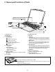
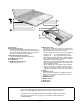
2 Names and Functions of Parts N G :LCD/Touchscreen H :Speaker I : LAN Port If the Mini Port Replicator is connected to the computer, connect the LAN cable to the LAN port on the Mini Port Replicator. You cannot use the LAN port on the computer. J : Modem Port Be sure to use the included modem telephone cable, and insert the end of the cable with the phyllite core into the modem port on the computer. K :Security Lock You can connect a Kensington cable. Refer to the instruction manual of the cable.
EXT. A :DC-IN Jack B :External Display Port If the Mini Port Replicator is connected to the computer, connect the external display to the external display port on the Mini Port Replicator. You cannot use the external display port on the computer. C :Mini Port Replicator Connector Connect the Mini Port Replicator (optional). D :SD Memory Card Slot E : PC Card Slot F : SD Memory Card Indicator Blinking: During access G :Microphone Jack A condenser microphone can be used.
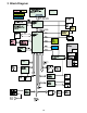
3 Block Diagram 10
4 Diagnosis Procedure 4.1.
4.2. Troubleshooting Please take note of the following two points with regard to troubleshooting: 1. Know-how of diagnosis upon occurrence of heavy troubles, e.g. Set cannot be turned ON , Set fails to start , No display on screen , etc. 2. Explanation of each trouble, mainly symptom of trouble in operation. Flow Chart START START Set cannot be supplied with current. Power lamp fails to light up. Pay attention to the following points when in pursuit of the cause of a troubleshooting. 1.
5 Power-On Self Test (Boot Check) Outline of POST The set has a boot check function called POST (Power-On Self Test) in it. The condition of the main body is diagnosed by checking beep sound or error code. Start .............Test begins automatically when power switch is set to ON. Normal finish .....After memory checking, a beep sound is issued once and the set is placed into automatic stop. Note: If no error occurs, nothing is displayed. (No display of OK, etc.
6 List of Error Codes The following is a list of the messages that BIOS can display. Most of them occur during POST. Some of them display information about a hardware device, e.g., the amount of memory installed. Others may indicate a problem with a device, such as the way it has been configured. Following the list are explanations of the messages and remedies for reported problems.
Troubleshooting 02D0 System cache error - Cache disabled Contact Panasonic Technical Support. 02F0: CPU ID: CPU socket number for Multi-Processor error. 02F4: EISA CMOS not writable ServerBIOS2 test error: Cannot write to EISA CMOS. 02F5: DMA Test Failed ServerBIOS2 test error: Cannot write to extended DMA (Direct Memory Access) registers. 02F6: Software NMI Failed ServerBIOS2 test error: Cannot generate software NMI (Non-Maskable Interrupt).
7 Self Diagnosis Test As for the self-diagnosis test(PC-Diagnostic utility) to use this model, a standard test and the enhancing test by the module of the main body building in are possible. Notes To skip BIOS password Use + key to skip BIOS password or authentication of fingerprint. This key is only for entering DIAG mode. Not available to boot the computer. If customer set "HDD Lock", the DIAG program cannot perform HDD test. *This key is for service purpose only.
2. Operation of PC-Diagnostic Utility -Only the device which can be inspected on the entire screen is displayed. -The item does not appear when the device of wireless LAN etc. is not physically connected. -The movement of the item must use an arrow key or a flat pad. -As for the device under the diagnosis, blue and yellow are alternately displayed at the left of the icon. - The diagnosis result of the device greens at the left of the icon when it is normal, and becomes red when abnormal.
2-1. Selection of tested device -To test only a specific device, "Test" and "Do not test" of each device can be selected. -The device which can select the enhancing test changes in order of "The standard is tested" and "Do not test" whenever the device icon is clicked. Do not test Start the standard test Please begin testing clicking if the selection of the tested device ends. 2-2.
7.1. Test Item and Division of trouble Test item Stanard Enhancing Content of standard test Content of enhancing test Place with possibility of breakdown CPU / SYSTEM CPU is shifted to protected mode, and "Violation of the paging", "Operation of the violation of a privileged instruction", and DMA, INT, TIMER, and the RTC operation are confirmed. CPU / Main board RAM All memory space is tested in a special memory access pattern based on "R.S.T . technology".
Test Item Standard Enhanced Content of Standard Test It is confirmed not to find abnormality in the USB connection of Touch Screen. This test cannot find abnormality of Touch Screen. It is confirmed not to find abnormality in the connection of Main board and Bluetooth module. It is confirmed not to find abnormality in the connection of Main board and Wireless WAN module. It is confirmed not to find abnormality in the legacy FD drive. This test cannot find abnormality of mechanical breakdown. (e.g..
8 Wiring Connection Diagram Connection Cable 1 LCD Cable 2 SP Cable 3 Antenna PCB-L 4 Antenna PCB-R 5 MODEM Cable 6 LAN Cable 7 PAD FFC 8 FPC Unit,HDD 9 DC-IN Cable 10 USB Cable Connection by Cable Direct connection Connectors Parts on Bottom Side Antenna Board (R) WWAN Antenna Board (R) LCD Unit and Touch Screen CN1501 Wireless LAN Module Battery Pack DFJS1050ZA DFJS962ZA N1ZYYY000002 N1ZYYY000003 DFJS973ZB DFJS958ZB DFJK12U112BB DL3UP1443AAA DFJS1020YA DFJS980ZA WWAN SIMM Card TS Board Keyboar
9 Disassembly instructions 9.1. Disassembly Flow Chart Main Unit 9.2.1. Preparation 1. End the Windows. 2. Turn off the Power, and then remove the AC Adaptor or Battery Pack. 3. Remove any optional DIMM Memory Cards or PCMCIA Cards. 4. Remove any other peripherals or Connected Devices. 9.2.2. Keyboard 9.2.3. Top Case 9.2.4. 9.2.5. LCD Open Knob /Speaker Touch Pad 9.2.7. 9.2.6. HDD USB Board 9.2.9 . 9.2.10. Antenna Board (L, R) / DC-IN 9.2.8. Main Board 9.2.11. W-LAN Board MDC MODEM 9.2.12.
9.1. Disassembly lnstructions 9.2.1. Preparation Attention: Before disassembly, be sure to perform the following steps. 1. End the Windows. 2. Turn off the power and then remove the AC adaptor. 3. Slide the hooks (A) and then remove the battery pack. 4. Remove the screw (A) and then remove the DIMM cover. (Remove if the DIMM memory is equipped with) Screw (A) : XSB2+4FNL (N16) 4. Remove the 6 hooks (B). 5. Open the keyboard from LCD side and then turn it inside out on the top case.
9.2.4. Removing the Top Case 9.2.3. Removing the HDD Preparation : perform the section 9.2.1., 9.2.2. first. 1. Remove the 2 screws (C) and then remove the HDD cover. Screw (C) : DFHE5025XA (N1) 2. Peel off the tape from HDD FPC. Tape : TPD-X0033A (S1001) Preparation : perform the section 9.2.1.,9.2.2. first. 1. Remove the 7 screws (D) and screws (E).
5. Lift up the top case and remove the pad FFC and then remove the top case. Top Case 9.2.5. Removing the Touch Pad Preparation : perform the section 9.2.1., 9.2.2. and 9.2.4. first. 1. Peel off the tape. Tape : DFHP7140ZA (K37) 2. Depress to center the 6 hooks of the pad cover, (C) (D) (E) as order. Tape Hook(D) Top Case Pad FFC Hook(F) PAD FFC Hook(E) Hook(F) 3. Remove the hook (F) and remove the touch pad.
9.2.6. Removing the LCD Knob and the Speaker Preparation : perform the section 9.2.1., 9.2.2. and 9.2.4. first. 1. Remove the latch spring from the top case. 2. Remove the hook of the LCD knob from stopper rib of the top case. 3. Peel off the4.Peel off the tape on the speaker and speaker ring and then remove the speaker. 9.2.8. Removing the Main Board Preparation : perform the section 9.2.1., 9.2.2. and 9.2.4. first. 1. Remove the 1 screw (I ), 1 screw (J), 2 screws (K) and 2 screws (L ).
9.2.9. Removing the Antenna Board (L,R) and the DC-IN Cable 6.Remove the LCD cable connectors (CN10,CN11). Preparation : perform the section 9.2.1., 9.2.2., 9.2.4. and 9.2.8. first. 1. Remove the antenna cable (L) from the main terminal and the antenna cable (R) from the AUX terminal and then remove the antenna board (L, R) from the bottom case. 2. Remove the DC-IN cable (CN600) from the main board. LCD Cable CN10 CN11 Antenna Board(L) Antenna Cable(L) CN600 DC-IN Cable 7.
9.2.11. Removing the MODEM Preparation : perform the section 9.2.1., 9.2.2., 9.2.4. and 9.2.8. first. 1. Remove the 2 screws (O). Screw (O) : DXQT2+D25FNL (N8) 2. Remove the MODEM from main board connector (CN18) as vertical. 2.Turn to the card bus ejector side. 3. Remove the 2 hooks (G) from the connector (CN14). Card Bus Ejector Hook (G) Main Board Screw (O) Screw (O) Modem CN14 CN18 9.2.13. Removing the LCD Unit 9.2.12. Removing the Card Bus Ejector Preparation : perform the section 9.2.1., 9.2.
9.2.15. Removing the LCD Unit and the LCD Rear 9.2.14. Removing the Hinge Cover Preparation : perform the section 9.2.1., 9.2.2., 9.2.4. and 9.2.13. first. 1. Remove the 2 screws (R) and then remove the hinge cover (L, R). Screw (R) : DRHM0108ZA (N1002) Screw (R) Preparation : perform the section 9.2.1., 9.2.2., 9.2.4. and 9.2.13. to 9.2.14. first. 1. Remove the 2 LCD Ruber and then remove the 2 screws (T). Screw (T) : DXHM0039ZA (N5) 2. Separate the LCD front and the LCD rear. 3.
9.2.17. Removing the WWAN Antenna Board (MAIN), (SUB) 9.2.18. Removing the WWAN Board / LCD Hook WAN Preparation : perform the section 9.2.1., 9.2.2., 9.2.4. and 9.2.13. to 9.2.15. first. 1. Open the SIMM cover and then remove the 2 screws (U). Screw (U) : DXHM0057ZA (N7) 2. Remove the antenna cover. Preparation : perform the section 9.2.1., 9.2.2., 9.2.4. and 9.2.13. to 9.2.15., 9.2.17. first. 1. Disconnect the WM cable from the connector (CN1501).
9.3. Reassenbly instructions 9.3.1. Attention when CF-T5L series is repaired - Please execute writing BIOS ID when you exchange the main board. - Parts (sheet and rubber) etc.related various the conductive cloth and heat spreader cannot be recycled.Use new parts. 9.3.2. Assembly knowhow of the LCD 9.3.2.1. Assembly of the LCD Front Does not run aground in a surrounding rib. -LCD Side Rubber, LCD Batt Rubber and LCD Magnet are not put out from the concave part.
9.3.2.3. Putting TP Flexible Protection Tape Sub-materials tape 30mm TP Flexible cable protection tape Upper : Near in the under putting of tape. Do not get on and do not go up. Right and left : It is matched to Flexible cable right edge. it does not overflow. Upper : The tape is matched to the edge of the glass. It does not overflow. Right and left : The tape is matched to Flexible cable’s right edge.It does not overflow. The tape is turned inside out.
9.3.2.5. Assembly of the LCD Unit LCD FRONT Lower and affix FRONT in parallel. TS Sub-materials tape 30mm The glass edge side match LCD resin frame The other side bottom match Do not go out to the back. LCD unit LCD resin frame The edge of the difference is matched. Flaking off paper 3 place removal FRONT TP CUSHION E LCD resin frame The edge of front externals is matched. LCD resin frame From externals 9.3.2.6. Assembly of the LCD Dumper Paste side Paste side It is thin.
wall affixation Affixation side The magnet is applied. LCD DAMPER A LCD DAMPER A It is affixed along the shape of the MAGNET. wall affixation wall affixation 9.3.2.7. Connecting LCD Cable The LCD cable is connected with the inverter. Wraps around the PET tape connector. The inverter is inserted in the inverter box and then affixes to rear case. LCD/inverter cable is connected. The connector is fixed with the tape of the inverter box.
ICD / Inverter Cable Connection Safety Work The flaking off paper is peeled off and then affixes on the connector. pressurizes by the finger. 9.3.2.8. Assembly of the Inverter and Putting Inverter Tapes A two sided tape of the Inverter Case bottom is peeled off, and put. Plinth externals standard Safety Work Inverter Case is arranged in the dotted line part.
Safety work Inverter Tape Affixes along shape Do not suppress the tab Safety work Rib root application Affixes along shape From the rib edge Safety work When INVTAPE is affixed on the LCD reception desk rib side, the treatment device is used. 9.3.2.9.
A red line of the cable is matched to the LCD frame externals 9.3.2.10. Putting PET Tape Two sided tape pressurizing The upper part of the LCD resin frame is matched. TP Flexible cable is bent once and the line is processed. Does not hang to the connector on LCD. TP TAPE 1mm or more The edge is matched and the substrate is affixed. TS substrate A Flexible cable connector right edge of the control substrate is matched to the inverter connector left end.
9.3.2.11. Line processing LCD cable (2) Sheet edge match After LCD Sheet is turned over and Conductive Cloth is put, a two sided tape is put. Safety work Conductive cloth All the signal lines are processed the conductive cloth internally. Connector Externals edge match Connector and conductive cloth wrapping part, it affixation is surely kicked.
The cable is prevented from The tape is distributed at the center and pasting applying. Safety work coming in succession mutually. Safety work The cable is prevented from running aground on the cushion. Put on the hinge surely. The remainder is put on the hinge side. LCD Damper C Gasket Cloth Externals match of plinth Externals match of reflector LCD Front is applied to the wall and pasting applying. Hinge-R Put the reflector part surely.
PET Tape Conductive Cloth (LCD Cable) The line is processed according to the LVDS cable. LCD insulator is matched to the edge. LCD Cable (Inverter part) LCD Cable Touch panels come most below. Moreover, the LCD cable comes. Damper LCD FRONT wall application affixation. FRAME externals are matched. Safety work The cable must not be processed on the damper,and give cable room. The line is processed according to the LVDS cable.
Pen Holder Holder Bottom Sheet Arranges match to the rib in the back of Pen Holder. Affixeson Holder Bottom Sheet. LCD Rear side standard (Convex of the hinge part is disregarded) The hole of the tape is matched to the hollow of the insertion part of the pen. Affixes from externals internally by 0.5mm or more. Pen Holder LCD Rear Pen Holder Tape 4.4mm The pressurizing time with the tool is 3 seconds or more.
9.3.2.14. Putting LCD Rear Cushions LCD REAR CUSHION LCD REAR CUSHION LCD REAR WAN 9.3.2.15. Assembly of the WM Cable Connector flat side Conductive cloth is wrapped. Black seat edge standard Black seat edge standard 3-7mm from Conductive cloth Filn Impedor is wrapped Film Impedr WM CABLE Conductive cloth Finished chart Overlap affixation of about 5mm 3-7mm from Conductive cloth Safety Work Pet Tape is wrapped.
9.3.2.16. Assembly of the WWAN Board LCD Hook Wan installation standard LCD Hook WAN The oreder of tightening screw (LCD Hook WAN) : The oreder of tightening screw (WWAN Board) : REAR wall application Screw Screw WWAN Board There is no order specification excluding a specified part. REAR wall application Screw WM Cable Connection 9.3.2.17.
A two sided tape of the cable after the cable position of Figure 1 is put out is affixed (cable fixation). The cable must not stretch. The convex part is matched to a black tape. PET TAPE (width L=30 of 19mm) Cable fixation 5-8mm Refer to Figure 1. 9.3.2.18.
Engages with LCD FRONT goods which have prepared LCD REAR Refer to Figure 1 Cable drawing out route The fingernail in four places is inserted PANASONIC LABEL Refer to Figure 2 ANTENNA COVER Safety work The LCD signal line is drawn out between wearing FRONT and REAR Insertion Lock engagement Multiply the fingernail in 16 all places surely Safety work The touch panel cable is drawn out between FRONT and HINGE.
9.3.2.20. Putting Productive Film Front panel On The space between the front panel and the touch panel surface is based on 0.8-1.2mm 0.2mm or more 0.2mm or more 0.2mm or more Productive Film 0.
9.3.3. Assembly knowhow of the Main Board 9.3.3.1. Putting tapes for Memory Sheet of top side Top side memory Sheet Bond neatly for the memory heat radiation purpose material Safety work It is confirmed that top side memory Sheet does not run aground on the switch. Board slit externals match 0 1mm There must not be running aground Board slit externals match 0 1mm Be sure to bond neatly for the memory heat radiation purpose material 9.3.3.2.
9.3.3.3. Putting PET tapes The order of tightening screw : Screw : DXQT2+D25FNL Processes on the capacitor Cable’s root is surely suppressed Processes next to the connector Screw A Tape Connector connection Processes between capacitors Affixes between DAI Screw B Processes to the CHIP set (CHIPSETDAI(Dotted line part) Thing that running aground is not in capacitor) Modem Cable must install MDC MODEM in Main Board after connects with MDC MODEM.
9.3.3.4. Assembly of the PCMCIA Ejector (Attention) Affixation load of affixation thing not instructed : More than 1kgf/c Main Board Screw Refer to < Explanation 1 > for the installation. The back of substrate The lever is drawn to Card Bus Ejector The lever is drawn to the the right before building in. left before building in. Square hole Bend < Explanation 1 > The sheet metal bend part of Main Board is inserted in the corner hole part.
9.3.3.6. Line processing LAN cable Thing to process modem cable previously 1.The modem cable is processed to the bottom ditch part. 2.
9.3.3.7. Assembly of the W-LAN Module / Putting Memory Sheet W-LAN MODULE (Attention) Affixation load of affixation thing not instructed : More than 1kgf/c Spreads on the terminal BATT (It is one blowing to the range) < Attention > Execute after setting the substrate in the receiving treatment device when working.
9.3.3.8. Putting Sheets (Attention) Affixation load of affixation thing not instructed : More than Pressurize More than 1-1.5 Connector externals application Management size : 0-1mm Grease(G-751) Heat Spreader Bottom Connector externals application Management size : 0-1m Connection Execute after setting the substrate in the receiving treatment device when working.
9.3.3.9. Assembly of the W-LAN Sheet W-LAN Sheet < preparation of W-LAN Sheet > W-LAN Sheet is the sheet metal externals and a difference match. W-LAN Sheet Runs side by side. The cutting lack part is inserted, and puts into the state of the roll. Horizontal direction is a suiting seat copper part externals 0-1mm. Sheet is lightly held by the finger and the fold habit is applied. The both sides tape flaking off paper is peeled off and affixes.
(Attention) Affixation load of affixation thing not instructed : More than 1kgf/c The white line is in respect Mountain case 6mm The white line is in respect Valley case 23mm Use the too Mountain case 35mm Use the too Valley case from white solid line on the back HDD FPC Valley case 45mm Bend completion chart PET Tape Watching confirmation of insertion in silk line Execute after setting the substrate in the receiving treatment device when working.
9.3.3.11. Assembly of the DC-IN Cable Ferrite Sheet Bends in the vicinity of the connector root. DC-IN Cable A It is confirmed to move right and left after wrapping. Bends in the vicinity of the tube root. Safety work B Do not give the terminal the load while working. (5) (5) 9.3.3.12. Setting the Main Board Insert HDD FPC in the opening of the bottom case while bent. No damage on the edge side to FPC. Confirm, and install the turning off position (left side) Main Board’s W-LAN SW.
9.3.4. Assembly knowhow of the Top Case 9.3.4.1. Assembly of the Speaker Soldering of Speaker Cable Affixation of Speaker Ring Solder must not overflow Board externals. Affix and kick according to the shape of the rib. Note not running aground in the rib. Speaker Ring Speaker Rib Soldering Soldering Solder must not overflow Board externals. Red line Black line Rib Speaker Cable Speaker installation Marking of the safety distance confirmation is put.
Safety Work 1 The cable is passed between bosses in the wall and the red circle part. There must not be slack. PET Tape Do not slacken from the tangent which connects the boss externals on the outside. < Speaker Cable processing > 0 2mm(Tape putting standard) Do not slacken from Cab standing wall by 3mm or more. Boss application 3 SPEAKER BOX SUNCALL is spread on the coloring part. Wall application (Attention) Affixation load of affixation thing not instructed : More than 1kgf/c 9.3.4.3.
9.3.4.4. Assembly of the LCD Knob Rib match (Gap 0.5mm or less) Sheet Put on the case before inserting the knob Confirm the LCD knob operates after installing the spring. Difference match (Gap 0.5mm or less) Spring KNOB and SRING are fixed The spring is hung. LCD Knob The hook is inserted while doing the slide. 9.3.4.5. Assembly of the Touch Pad Affixation of PAD Cover Tape It is a thing which does not run PAD Cover PAD aground in the pin as for the Cover Tape PAD button seat.
MINI-PCI Cushion The gap is 0.5mm or less. FFC bend specification Insert and put a round pin of the lens on U ditch of the cushion.
9.3.5. Assembly knowhow of the Bottom Case 9.3.5.1. Setting Antenna Board and Line processing (1) Wiring of Antenna Cable (L) Process Antenna Cable (L) which remained after installing Antenna Board (L) in the Bottom Case as shown in the figure below. Safety work Processes with the boss between ribs Safety work Boss DC-IN is installed in bottom Places between the Bottom Case and installs Safety work Ferrite sheet is processed in board. The load is not put on the terminal of DC-IN.
9.3.5.3. Line processing LAN Cable / USB Cable / MODEM Cable Sheet Put the Sheet to Bottom Rib (In the rib edge side match, to the bottom. ) Sub Board Bottom Rib LAN Cable ANT Cable 8mm MODEM Cable Safety work 5mm Safety work USB Cable 1mm or more Along the bottom bottom of the ANT cable, and process the line with the PET tape. If the ANT cable had processed the tape, the position is arbitrary.
9.3.6. Assembly knowhow of the Body 9.3.6.1. Setting LCD LCD UNIT SCREW(a) DXQT26+D5FNL SCREW(b) DXQT26+D5FNL Safety work Conductive Cloth is wrapped. 9.3.6.2. Line processing LCD Cable (bottom case side) Work is executed in order of (1) (2) (3) (4). TP Cable Fix Sheet TP Cable Fix Sheet Safety work Affixes to the wall at bottom by the rib match. The final state 60 3mm Conductive Cloth Safety work 4 8mm The seat is rolled to cover the cable, and puts on the hinge wall.
Safety work The TP cable must not run aground in the boss. TP cable Connector connection Safety work The tape is pasted from the upper surface of DC Jack Holder to the side and the TP Cable is fixed. It is confirmed that the TP Cable is not a file. The TP cable is fixed by drawing line processing Sheet in the direction of the arrow. Line Hold Sheet Direction of cable drawing Safety work The edge of the tube of the TP cable must reached the DC Jack Holder. The cable passes the route of this line. 9.3.
9.3.6.4. Putting Line Hold Sheet WWAN Lower flaking off paper is taken beforehand, and Line Hold Sheet WWAN is pasted to the relay cable according to remaining flaking off paper. Afterwards, Sheet is arranged in Bottom Case. Line Hold Sheet WWAN is inserted in space in the interior of the Bottom Case. Safety work The flaking off paper is taken, and a two sided tape is folded and pasted to the Bottom. The relay cable is pushed into the bottom. The slack of the line is processed on the right side.
9.3.6.6. Assembly of the Keyboard Heat Sheet’s KB (largeness) affixation Heat Sheet KB(largeness) Keyboard Edge side match of keyboard hole Inclination 0.5mm or less Inclination 0.5mm or less Edge side match of keyboard hole KB Plate / KB Plate Sheet /Tape affixation 1.KB Plate assembly 2.Both sides tape affixation Tape Concave side KB Plate KB Plate Sheet 3.
9.3.6.7. Assembly of the Heat Spreader and Side Cover R A remaining tape is affixed on an opposite side Grease (G-751) is spread Safety work PET Tape Heat Spreader(Top Case Side) (Note) When the part of aluminum with a thin all surroundings bends, Sheet and the cable might be damaged.Therefore, correct when bending. However, correct without correcting by barehanded with a tool such as pliers.
The fingernail is multiplied. Suppresses and installs the direction of the arrow after the connector part is inserted . DDR2 MicroDIMM Screw A (XSB2+4FNL) is tightened. DIMM Cover Screw A 9.3.6.10. The tightening screw of Bottom Case The Keyboard is inserted and after tightening of the Screw, the Keyboard Hook are inserted in order of the following. 1.7 Screws A (DXHM0039ZA) are tightened. 2.5 Screws B (DXHM0057ZA) are tightened. 3.3 Screws C (DXQT2+E12FNL) are tightened. 4.
9.3.6.11. Putting Sheets Bottom Sheet USA Affixed to the concave part (Exist in the concave part) The label floatage and the bubble are prevented from being. Pasting applying standard Space of 5mm in surroundings Bottom Backup Sheet Pasting according to the corner Bottom Sheet USA1 Product number : T1207Z Product number : T1206Z Safety work Safety work Battery Sheet Tape affixation on corner side in end match of R Do not overflow up (Gap 1mm or less) The edge is matched.
9.3.6.12. Setting Knobs Bottom Case Power Knob Left justify Left justify LAN SW Knob CF-T5*C**** is not used 9.3.6.13. Putting RJ Cover and Labels RJ Cover Safety work RJ Cover is put on the denting part. The paste is prevented from protruding beyond the edge side. The cover is prevented from protruding beyond the denting part. The cover is prevented from running aground from the denting part. It is not possible to recycle.
Bottom Sheet USA COA Label The COA label matches and puts externals of Bottom Sheet. Laminate seal The lamination seal sets the direction of Microsoft of polo gram character in the direction of the character of the label. Model Label Bottom Sheet USA1 Revision Label 9.3.6.14. Assembly of the HDD / HDD Cover HDD Case WAN HDD PET Tape Edge of side putting rubber Puts on the lid of the HDD Case with the PET Tape.
9.3.6.15. Putting HDD Cover Heat Sheet and Bottom Heat Sheet HDD Cover Heat Sheet The left end and the top are set to the concave part of the cover and HDD Cover Heat Sheet is put. Do not overflow. Inclination 1mm or less SCREW (DXQT26+D8FCL) Bottom Heat Sheet Handy Strap Bottom Heat Sheet puts Label according to a right edge and the top. Do not overflow. Inclination 1mm or less SCREW (DXQT26+D8FCL) Handy Strap Angle Handy Strap Angle It is noted not to mistake the back for the table of Angle.
9.3.6.16. Putting Tapes for WWAN Antenna Cable After the module is tested, the following work is executed. SCREW (DFHE5025XA) Line Hold Sheet The point part of the cable is fixed. However do not paste the tape on the connector. SCREW (DFHE5025XA) 9.3.6.17. Assembly of the LCD Rear SIMM cover is opened. Screw(DXHM0057ZA) are tightened. (Reuse) LCD Unit A B Antenna Cover (A) The fingernail in the point part is inserted. (B) This side is lowered and then engages. Screws (DXHM0039ZA) are tightened.
9.3.6.18. Assembly of the WWAN Module Safety work Edge Guard Tape is put on the point of 1mm on the edge of the module land. Hide the side of the shield board in the module after the Edge Guard Tape putting. Edge Guard Tape is put. Antenna connector connection Cable Fixed Sheet SCREW (DFHE5025XA) After the module is inserted and then the screws are tightened. The card shall be inserted and separated correctly according to the direction and the process as shown below.
10 Exploded View 10.1.
10.2.
10.3.
10.4.
12 Replacement Parts List Note : Important Safety Notice Components identified by mark have special characteristics important for safety. When replacing any of these components, use only manufacturer's specified parts. CF-T5LWETZBM REF. NO and AREA Main Block Unit E1 E2 E3 E4 E5 E6 E7 E8 E9 E10 E11 E12 E13 E14 E15 E17 E18 E19 E20 E21 E22 E1010 E1010-1 E1010-1-1 E1010-1-1-1 E1010-1-2 E1010-1-3 E1010-1-4 E1010-1-5 E1010-1-6 E1010-2 E1023 E1024 E1025 E1026 E1027 Accessories A1 A2 PART NO.
A3 A4 A5 A6 A7 A8 Packing Material P5 P6 P7 Mechanical Parts K1 K2 K3 K4 K5 K6 K7 K8 K10 K11 K12 K13 K14 K15 K16 K17 K18 K19 K20 K21 K24 K26 K30 K31 K32 K35 K36 K37 K41 K42 K43 K44 K45 K46 K47 K48 K49 K50 K51 K53 K54 CGR-B/979A DFQX5616ZA DFHR9081XA DFME0148ZA DFJS1070ZA DFHS9017ZA LITHIUM ION BATTERY PACK(9CELL) MANUAL(CF-T5MK1) PEN TETHER T4 MODEM CABLE TOUCHPANEL FUKINUNO 1 1 1 1 1 1 DFPK1194YA DFPN0833ZA DFPN0846ZA PACKING CASE(OVERSEAS) CUSHION B CUSHION T 1 2 2 DFBC0321ZA-0 DFBD0180ZB-0 DFBD018
K55 K56 K57 K59 K60 K61 K63 K64 K67 K68 K69 K70 K71 K72 K74 K75 K76 K77 K78 K79 K80 K81 K82 K83 K84 K85 K87 K89 K90 K91 K1001 K1002 K1003 K1004 K1005 K1010 K1011 K1013 K1014 K1015 K1016 K1017 K1018 K1019 K1020 K1021 K1022 K1023 K1024 K1025 K1026 K1027 DFKE0772ZA-0 DFKE0877ZA-0 DFKE0878ZA-0 DFQT6342ZA DFMY3231ZA DFMY0432ZA DFKE0783YA-0 DFKF0274ZA-0 DFKM0523ZA-0 DFKM8172UA-0 DFMD1203ZA DFMD3121ZA DFMD4057ZA DFMD7A52ZA DFMX0635ZB DFMX1155ZA DFMX1160ZA DFMX1184ZA DFMX1262ZA DFMY0399ZA DFMY0421ZA DFMY3191YA DFM
K1028 K1029 K1030 K1031 K1035 K1036 K1038 K1039 K1039-1 K1040 K1041 K1042 K1043 K1046 K1047 K1048 K1049 K1050 K1051 K1052 K1053 K1054 N1 N2 N4 N5 N6 N7 N8 N9 N10 N11 N12 N13 N14 N15 N1001 N1002 N1003 S1001 S1002 DFHR3E92ZA DFHR5484ZA DFHR8526ZA DFKE0815ZA-0 DFKE0879ZA-0 DFKE0884ZA-0 DFKF0275ZB-0 DFKF8166XA-0 DFHG371ZA-1 DFKH1020ZA-0 DFMD1191YA DFMX0904ZA DFMX1251ZA DFGT1206ZA DFGT1207ZA DFHE0463ZA DFHE0862ZA DFHE1035ZA DFHP7272ZA DFHR3154ZA DFHR3F84ZA DFQX3998XA DFHE5025XA DFHE5035ZB DRQT2+G6FKL DXHM0039ZA
Replacement Parts List Note: Important Safety Notice Components identified by mark have special characteristics important for safety. When replacing any of these components use only manufacturer's specified parts. CF-T5LWETZBM (06-10-27) REF. NO and AREA MAIN PCB C 3 PART NO. DESCRIPTION Q'TY F1J0J226A051 CAPACITOR, 6.3V, 22µF 8 EEFCX0D221R CAPACITOR, 2V, 220µF 6 F1G1C104A042 CAPACITOR, 16V, 0.
C 135 C 136 C 137 C 142 C 143 C 144 C 145 C 146 C 147 C 148 C 168 C 169 C 171 C 175 C 177 C 178 C 180 C 182 C 183 C 187 C 188 C 189 C 190 C 191 C 192 C 193 C 194 C 195 C 196 C 197 C 198 C 199 C 200 C 201 C 202 C 203 C 204 C 205 C 207 C 208 C 209 C 217 C 219 C 221 C 222 C 228 C 257 C 258 C 259 C 260 C 262 C 275 C 283 C 289 C 290 C 291 C 292 C 293 C 294 C 295
C 296 C 298 C 305 C 310 C 311 C 313 C 314 C 315 C 316 C 317 C 318 C 319 C 321 C 323 C 326 C 328 C 332 C 347 C 351 C 358 C 364 C 375 C 377 C 378 C 379 C 383 C 384 C 386 C 392 C 393 C 394 C 406 C 413 C 420 C 430 C 431 C 434 C 435 C 436 C 437 C 438 C 442 C 445 C 604 C 609 C 639 C 641 C 674 C 717 C 45 C 48 C 58 C 59 C 62 C 63 C 70 C 72 C 74 C 87 C 93 F1J0J106A016 CAPACITOR, 6.
C 167 C 176 C 206 C 280 C 297 C 303 C 304 C 325 C 339 C 368 C 395 C 441 C 446 C 447 C 668 C 695 F1G1E103A062 CAPACITOR, 25V, 0.01µF 21 C 49 F1G1H222A496 CAPACITOR, 50V, 2200pF 1 C 53 F1G1A104A014 CAPACITOR, 10V, 0.
C 116 C 117 C 130 C 131 C 132 C 133 C 138 C 139 C 140 C 141 C 172 C 173 C 184 C 186 C 214 C 216 C 301 C 322 C 338 C 346 C 390 C 399 C 606 C 694 C 702 C 73 F1G1A474A018 CAPACITOR, 10V, 0.47µF 4 F1J0J4750019 CAPACITOR, 6.3V, 4.7µF 11 F1H0J1050022 CAPACITOR, 6.3V, 1µF 11 F1G1H3R3A543 CAPACITOR, 50V, 3.
C 667 C 683 C 686 C 181 EEFSX0D331ER CAPACITOR, 2V, 330µF 5 F1G1H100A544 CAPACITOR, 50V, 10pF 8 C 676 C 698 C 708 C 709 C 210 C 211 C 212 C 404 C 415 C 416 C 418 C 419 C 223 EEFUD0J151ER CAPACITOR, 6.3V, 150µF 1 C 224 EEFCX0J101R CAPACITOR, 6.
C 287 C 288 C 263 F1J1A1050021 CAPACITOR, 10V, 1µF 1 C 264 F1G0J224A001 CAPACITOR, 6.3V, 0.22µF 7 F1G1H1010005 CAPACITOR, 50V, 100pF 8 F1G1H5R0A543 CAPACITOR, 50V, 5pF 2 C 265 C 333 C 334 C 335 C 336 C 366 C 306 C 307 C 362 C 363 C 385 C 615 C 664 C 691 C 320 C 324 C 329 F1L3D102A003 CAPACITOR, 2000V, 1000pF 1 C 354 F1L0J107A016 CAPACITOR, 6.3V, 100µF 2 F1G1H471A496 CAPACITOR, 50V, 470pF 2 C 356 C 367 C 439 C 400 F1G1A683A014 CAPACITOR, 10V, 0.
F1H1H103A748 CAPACITOR, 50V, 0.01µF 2 F1G1H221A495 CAPACITOR, 50V, 220pF 8 F1J0J475A009 CAPACITOR, 6.3V, 4.7µF 5 EEFCX0G151R CAPACITOR, 2V, 150µF 2 F1G1C473A004 CAPACITOR, 16V, 0.047µF 3 C 642 F1G1H121A495 CAPACITOR, 50V, 120pF 1 C 643 F1G1H561A496 CAPACITOR, 50V, 560pF 1 C 645 F1H1H1830001 CAPACITOR, 50V, 0.018µF 1 C 646 F1G1H182A496 CAPACITOR, 50V, 1800pF 1 C 650 F1J1H224A533 CAPACITOR, 50V, 0.
D 6 D 7 B0ADDH000004 DIODE 6 B3ABB0000164 LED 4 D 8 D 9 D 601 D 602 D 604 D 10 D 11 D 12 D 13 D 15 B3AKB0000008 LED 1 D 16 B3ACB0000020 LED 2 D 20 B3ABB0000274 LED 1 D 23 MA2S111-TX DIODE 3 B0JCPD000023 DIODE 3 D 605 MAZ81200ML DIODE 1 D 606 MAZ81800ML ZENER DIODE 1 D 607 MA3S132E0L DIODE RECTIFIER 2 D 21 D 619 D 621 D 600 D 603 D 636 D 622 D 608 B0JCQD000001 DIODE 1 D 609 B0JCMD000014 SHOTKEY BARRIER DIODE 7 B0JDAE000004 DIODE 2 MAZ80510ML DIODE 6 D 611
IC 10 IC 11 IC 12 IC 13 C0JBZZ000388 IC, CLOCK GENERATOR 1 IC 16 C0CBCBG00008 IC, REGULATOR 1 IC 17 C1DB00001182 IC, LAN CONTROLLER 1 IC 18 C3EBCG000100 IC, EEPROM 1 IC 19 C0CBCBC00137 IC, REGURATOR 1 IC 20 C1CB00002540 IC, TEMPERATURE CENSOR IC 1 IC 21 C0DBZYY00026 IC, USB POWER SW 3 C0JBAR000515 IC, Q-SWITCH 2 IC 22 IC 71 IC 27 IC 29 IC 28 C0DBZYY00016 IC 1 IC 30 C1CB00002449 IC, AUDIO CODEC 1 IC 31 C0CBCBC00181 IC 1 IC 33 C1CB00002268 IC, SECURITY CHIP 1 IC
L 5 J0JHC0000074 INDUCTOR 4 J0JCC0000186 INDUCTOR 9 J0JBC0000072 INDUCTOR, FILTER 3 J0ZZB0000080 IDUCTOR, COMMON MODE FILTER 2 L 7 L 26 L 54 L 13 L 14 L 27 L 28 L 29 L 30 L 31 L 32 L 33 L 17 L 18 L 19 L 21 L 22 L 25 DDB5Z024E-L INDUCTOR 1 L 34 DDB5Z024C-L IDUCTOR, FERRITE PARTS 4 DDB5Z021C-Y INDUCTOR 6 DDB5Z032A-L INDUCTOR, FERRITE PARTS 2 L 35 L 36 L 37 L 38 L 39 L 40 L 41 L 42 L 43 L 55 L 56 L 57 J0MAB0000116 INDUCTOR, EMI FILTER 1 L 601 G1C4R7MA0022 INDUCTOR 3 L 608 G1
Q 6 B1CFGD000023 TRANSISTOR 8 XP0421300L TRANSISTOR 9 B1DHDC000028 TRANSISTOR 4 B1MBDCA00004 TRANSISTOR 3 B1GBCFNN0042 TRANSISTOR 7 XP0421400L TRANSISTOR 3 Q 7 Q 27 Q 647 Q 654 Q 662 Q 663 Q 666 Q 10 Q 36 Q 38 Q 628 Q 631 Q 632 Q 634 Q 635 Q 636 Q 11 Q 40 Q 630 Q 633 Q 28 Q 35 Q 37 Q 29 Q 54 Q 601 Q 603 Q 605 Q 611 Q 624 Q 46 Q 47 Q 600 Q 48 B1GFCFEN0003 TRANSISTOR 1 Q 53 B1GBCFNL0017 TRANSISTOR 1 Q 602 B1CFMC000008 FET 1 Q 607 B1CHRD000001 FET 2 B1DHFD000015 TRANSISTOR
R 187 R 218 R 235 R 272 R 273 R 392 R 393 R 462 R 479 R 480 R 492 R 2 ERJ2GEJ510X RESISTOR, 1/16W, 51Ω 4 ERJ2GEJ101X RESISTOR, 1/16W, 100Ω 25 ERJ2RKF1001X RESISTOR, 1/16W, 1KΩ 2 R 5 R 6 R 9 R 13 R 14 R 65 R 203 R 237 R 332 R 350 R 362 R 391 R 478 R 486 R 502 R 504 R 508 R 518 R 608 R 609 R 667 R 668 R 673 R 676 R 677 R 678 R 679 R 697 R 15 R 696 R 16 ERJ2RKF2001X RESISTOR, 1/16W, 2KΩ 1 R 18 ERJ2RKF51R0X RESISTOR, 1/16W, 51Ω 1 R 19 ERJ2RKF27R4X RESISTOR, 1/16W, 27.
R 31 ERJ2GEJ562X RESISTOR, 1/16W, 5.6KΩ 6 ERJ2RKF2210X RESISTOR, 1/16W, 221Ω 2 ERJ2RKF1000X RESISTOR, 1/16W, 100Ω 3 R 354 R 610 R 614 R 616 R 747 R 37 R 39 R 38 R 40 R 42 R 41 ERJ2RKF2000X RESISTOR, 1/16W, 200Ω 1 R 63 ERJ2RKF1002X RESISTOR, 1/16W, 10KΩ 1 R 66 ERJ2GEJ222X RESISTOR, 1/16W, 2.2KΩ 7 ERJ2RKF80R6X RESISTOR, 1/16W, 80.6Ω 2 D1H81034A024 RESISTOR ARRAY 7 R 384 D1H84734A024 RESISTOR ARRAY 1 R 79 ERJ2GEJ390X RESISTOR, 1/16W, 39Ω 2 ERJ2RKF1501X RESISTOR, 1/16W, 1.
R 372 R 374 R 396 R 402 R 413 R 421 R 422 R 426 R 428 R 437 R 444 R 447 R 448 R 452 R 453 R 484 R 519 R 520 R 521 R 619 R 639 R 644 R 688 R 704 R 708 R 712 R 713 R 728 R 733 R 734 R 743 R 817 R 95 ERJ2GEJ201X RESISTOR, 1/16W, 200Ω 4 D1HG1008A001 RESISTOR ARRAY 8 ERJ2GEJ100X RESISTOR, 1/16W, 10Ω 37 R 96 R 97 R 98 R 99 R 100 R 101 R 102 R 127 R 128 R 129 R 130 R 103 R 104 R 105 R 106 R 107 R 108 R 109 R 110 R 111 R 112 R 113 R 114 R 115 R 116 R 117 R 118
R 119 R 120 R 121 R 122 R 123 R 124 R 125 R 126 R 341 R 636 R 637 R 649 R 650 R 705 R 706 R 716 R 717 R 725 R 726 R 737 R 738 R 131 R 132 R 133 R 134 R 135 R 136 R 137 R 138 R 139 R 140 R 141 R 142 R 143 R 144 R 145 R 146 R 147 R 148 R 149 R 150 R 151 R 152 R 153 R 154 R 155 R 156 R 189 R 192 R 224 R 226 R 233 R 238 R 239 R 240 R 247 R 252 R 257 R 316 R 317 ERJ2GE0R00X RESISTOR, 1/16W, 0Ω 68
R 333 R 346 R 386 R 399 R 406 R 407 R 430 R 431 R 449 R 450 R 458 R 472 R 481 R 485 R 487 R 491 R 501 R 600 R 692 R 703 R 719 R 760 R 761 R 763 R 768 R 773 R 774 R 785 R 787 R 157 D1HA56080001 RESISTOR ARRAY 7 ERJ2GEJ104X RESISTOR, 1/16W, 100KΩ 31 R 158 R 159 R 160 R 161 R 162 R 163 R 165 R 171 R 215 R 248 R 249 R 250 R 308 R 311 R 331 R 334 R 337 R 342 R 343 R 352 R 383 R 454 R 459 R 460 R 461 R 475 R 476 R 503 R 506 R 611
R 621 R 623 R 624 R 625 R 664 R 666 R 672 ERJ3GEYJ1R0V RESISTOR, 1/16W, 1Ω 8 ERJ2GEJ472X RESISTOR, 1/16W, 4.
R 221 ERJ2GEJ470X RESISTOR, 1/16W, 47Ω 4 R 222 R 443 R 473 R 229 ERJ2RKF22R6X RESISTOR, 1/16W, 22.6Ω 1 R 246 ERJ3GEYJ121V RESISTOR, 1/16W, 120Ω 1 R 255 ERJ2GEJ334X RESISTOR, 1/16W, 330KΩ 3 R 258 ERJ2GEJ203X RESISTOR, 1/16W, 20KΩ 1 R 259 ERJ2GEJ106X RESISTOR, 1/16W, 10MΩ 1 R 260 ERJ2GEJ105X RESISTOR, 1/16W, 1MΩ 6 ERJ2GEJ363X RESISTOR, 1/16W, 36KΩ 2 R 305 ERJ2RKF3922X RESISTOR, 1/16W, 39.
R 605 ERJ2RHD104X RESISTOR, 1/16W, 100KΩ 2 ERJ2RKD154X RESISTOR, 1/16W, 150KΩ 2 ERJ1TYJ331U RESISTOR, 1W, 330Ω 2 R 613 R 606 R 612 R 615 R 617 R 618 ERJ3GEYJ3R3V RESISTOR, 1/16W, 3.3Ω 1 R 628 D1BDR1000002 RESISTOR, 1/8W, 0.1Ω 1 R 626 RL1220SR15F RESISTOR, 1/8W, 0.15Ω 2 D1BDR0220001 RESISTOR, 1/8W, 0.
R 689 ERJ2RKF1003X RESISTOR, 1/16W, 100KΩ 1 R 690 ERJ2RKF1800X RESISTOR, 1/16W, 180Ω 1 R 693 ERJ2RKF1801X RESISTOR, 1/16W, 1.80KΩ 1 R 694 ERJ2RKF4701X RESISTOR, 1/16W, 4.7KΩ 2 R 710 R 695 ERJ2RKF4221X RESISTOR, 1/16W, 4.22KΩ 1 R 700 D1ZZ00000093 RESISTOR, 1W, 1mΩ 1 R 711 ERJ2RKF1502X RESISTOR, 1/16W, 15KΩ 2 R 714 ERJ2RKF5102X RESISTOR, 1/16W, 51KΩ 1 R 715 ERJ2RKF2402X RESISTOR, 1/16W, 24KΩ 1 R 721 D1BDR0470002 RESISTOR, 1/8W, 0.
C 1112 C 1113 C 1110 F1G1E223A062 CAPACITOR, 25V, 0.022µF 1 C 1101 F1G1E472A062 CAPACITOR, 25V, 4700pF 4 C 1102 C 1103 C 1104 C 1111 F1G1H102A450 CAPACITOR, 50V, 1000pF 1 C 1114 F1G0J224A001 CAPACITOR, 6.3V, 0.22µF 1 C 1115 F1J0J475A009 CAPACITOR, 6.3V, 4.7µF 1 C 1116 F1J0J106A024 CAPACITOR, 6.
CN 1502 K1MY52BA0190 MINI-PCI-EXP CONNECTOR 1 CN 1503 K1NA08E00007 CONNECTOR 1 D 1520 DEDRB081L20 DIODE 1 IC 1520 C0DBAYY00204 IC, DC/DC CONVERTER 1 1 L 1520 G1C2R7MA0273 INDUCTOR, COIL Q 1520 B1CFGD000023 TRANSISTOR 1 Q 1522 B1DHFD000015 TRANSISTOR 1 Q 1521 B1GBCFNN0042 TRANSISTOR 1 R 1502 ERJ2GEJ101X RESISTOR, 1/16W, 100Ω 2 ERJ2GE0R00X RESISTOR, 1/16W, 0Ω 2 ERJ2GEJ103X RESISTOR, 1/16W, 10KΩ 2 R 1522 D1BDR0330001 RESISTOR, 1/8W, 0.