
Data Sheet
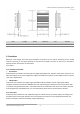
Table Of Contents

LoRa Concentrator Card_GL5712-UX_Datasheet_V1.0.0
Shenzhen Zaina Technology Co.,Ltd - 2 -
Table3.1 General specification
2.2 Electric specifications
ESD Notice: GL5712-UX is a high performance radio frequency device. It satisfies:
Class 2 of the JEDEC standard JESD22-A114 (Human Body Model) on all pins.
Class III of the JEDEC standard JESD22-C101 (Charged Device Model) on all pins
It should thus be handled with all the necessary ESD precautions to avoid any permanent damage.
The limiting values given are in accordance with the Absolute Maximum Rating System (IEC 134). Stress
above one or more of the limiting values may cause permanent damage to the device. These are stress
ratings only, and operation of the device at these or at any other conditions above those given in the
Characteristics sections of the specification is not implied. Exposure to these limits for extended periods
may affect device reliability.
2.3 Absolute maximum rating
Table2.3 absolute maximum rating
Stressing the device beyond the “Absolute Maximum Ratings” may cause permanent damage. The
product is not protected against over-voltage or reversed voltages. If necessary, voltage spikes
exceeding the power supply voltage specification, given in table above, must be limited to values within
the specified boundaries by using appropriate protection diodes.
2.4 Operating conditions
All specifications are at an ambient temperature of 25°C. Extreme operating temperatures can
significantly impact specification values. Applications operating near the temperature limits should be
tested to ensure the specification.
Symbol Description Condition
Min
Max.
Unit
3.3Vaux
Module supply
voltage
Input DC voltage at 3.3Vaux pins –0.3 3.6
V
USB
USB D+/D- pins Input DC voltage at USB interface pins
3.6
V
SPDT_SEL Port select Input DC voltage at SPDT_SEL input pins
–0.3 3.6
V
RESET MPCI reset input Input DC voltage at RESET input pin –0.3 3.6
V
SPI SPI interface Input DC voltage at SPI interface pin –0.3 3.6
V
GPS_PPS GPS 1 pps input Input DC voltage at GPS_PPS input pin –0.3 3.6
V
Rho_ANT Antenna ruggedness
Output RF load mismatch ruggedness at
ANT1
10:1
VSWR
Tstg Storage Temperature
–40 85 °C