
Datasheet


71M6xxx Data Sheet
17
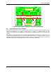
4.7 IC Pinout
VCC TEST
SP
SN
GND NC
INP
INN
1
2
3
4
5
6
7
8
Figure 9: Pinout for 8-Pin SO Package
4.8 Pin Description
Table 12: Pin Description
PIN
NAME
FUNCTION
1
VCC
Supply Voltage Output. A 1.0
µ
F capacitor to GND should be provided.
2 SP
Positive Bidirectional Communication Port for the Connection of the Pulse
Transformer
3 SN
Negative Bidirectional Communication Port for the Connection of the Pulse
Transformer
4 GND
Ground (Local Ground). The voltage at the INP and INN pins references to
this pin.
5
NC
No Connection. No connections must be made to this pin.
6 INP
Positive Analog Input from Sensor. This input must be biased towards
GND with a 1k
Ω
resistor.
7 INN
Negative Analog Input from Sensor. This input must be biased towards
GND with a 1k
Ω
resistor.
8 TEST
Input Used in Factory for Test Purposes. This pin must be connected to
GND.