
Datasheet


71M6xxx Data Sheet
4
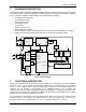
1 HARDWARE DESCRIPTION
The 71M6103/71M6113/71M6201/71M6203/71M6601/71M6603 (71M6xxx) remote sensor ICs integrate
all functional blocks required to implement an isolated front-end with digital communication capability.
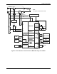
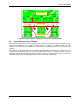
Figure 1 shows the 71M6xxx IC block diagram. The chip includes the following:
• Preamplifier with a fixed gain
• 22-bit delta-sigma ADC
• ADC voltage reference
• Temperature sensor
• VCC monitor
• Power-on reset circuitry
• Bidirectional pulse interface
• Active rectifiers for supply-voltage generation from the power pulses provided by the 71M654x
• Digital control section providing control registers for the selection of operation modes
SP
SN
PLL
PULSEIO
Secondary
ACTIVE
RECTI-
FIERS
GND VCC
RD_DATA
DIGITAL SECTION
INP
INN
ADC
ADC_CLK
ADC_OUT
BAND
GAP
CHOP
+
IBIAS
TEMP/VCC
MONITOR
OTP MEMORY
BUFFER
VREF
VBIAS
TEST
DATA_IN[15:0]
CROSS
VCC
WR_DATA
POWER
ON
RESET
RESET
RD_CLK
VDD
RD_DATA
PREAMP
+
-
-
Primary
1:1.1
To
71M654X
SHUNT
Figure 1: Block Diagram
2 FUNCTIONAL DESCRIPTION
During normal operation, the SP and SN pins of the 71M6xxx are connected to the pulse transformer.
When PLL_FAST = 1 in the 71M654x, power pulses generated by the 71M654x arrive every 610.35ns.
The PLL in the 71M6xxx locks to these incoming power pulses. The communication between the
71M654x and the 71M6xxx is synchronized to the multiplexer frames of the 71M654x. The
communication protocol is Maxim Integrated-proprietary, and details are not described in this data sheet.
All aspects of the communication between the 71M654x and the 71M6xxx are managed on the hardware
level and they are completely transparent to the user.
The communication interface can run at two different data rates. Power pulses are generated every
610.35ns if the PLL_FAST register in the 71M654x is set to 1, and every 1.905µs if PLL_FAST is set to 0.
The power pulses are 101.7ns wide with PLL_FAST = 1, and 160ns wide with PLL_FAST = 0.