
Datasheet


71M6xxx Data Sheet
9
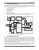
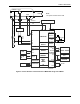
MPU
RTC
TIMERS
IADC0
VADC8 (VA)
IADC2
VADC9 (VB)
XIN
XOUT
RX
TX
TX
RX
COM0...5
V3P3A V3P3SYS
VBAT
VBAT_RTC
IADC4
VADC10 (VC)
SEG
GNDA GNDD
SEG/DIO
DIO
ICE
C
B
A
NEUTRAL
LOAD
8888.8888
PULSES,
DIO
IR
AMR
POWER FAULT
COMPARATOR
MODUL-
ATOR
SERIAL PORTS
OSCILLATOR/
PLL
MUX and ADC
LCD DRIVER
DIO, PULSES
COMPUTE
ENGINE
FLASH
MEMORY
RAM
32 kHz
REGULATOR
Shunt Current Sensors
POWER SUPPLY
71M6543F/
71M6543H
TEMPERATURE
SENSOR
VREF
IADC6
BATTERY
PWR MODE
CONTROL
WAKE-UP
NEUTRAL
I
2
C or µWire
EEPROM
9/17/2010
IADC1
IADC3
IADC5
IADC7
RTC
BATTERY
V3P3D
BATTERY
MONITOR
SPI INTERFACE
HOST
LCD DISPLAY
Resistor Dividers
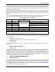
Pulse Transformers
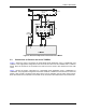
3x 71M6xx3
Note: This system is referenced to Neutral
71M6xx3
71M6xx3
71M6xx3
}
IN*
}
IA
}
IB
}
IC
*IN = Neutral Current
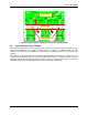
Figure 4: Current Sensors Connected to the 71M6543F/H or 71M6545/H with Three 71M6xx3
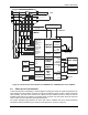
3.4 PCB Layout Considerations
To limit emissions and susceptibility to electromagnetic and magnetic fields, the signal wiring between the
shunt resistors and the 71M6xxx should be as short as possible and should consist of tightly twisted pair
cable. Similarly, the PCB traces between the 71M6xxx and the 71M654x should be routed as short as
possible and should be surrounded by grounded copper structures. The trace pairs should be routed as
close to each other as permitted by the PCB manufacturer.
The copper separation (gap) between the shunt side and the 71M654x side of the signal transformer
should be as wide as permitted by the footprint of the transformer, as shown in Figure 5.