
Datasheet

71M6521DE/DH/FE Data Sheet
Rev 3 Page: 103 of 107
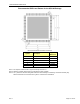
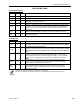
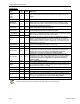
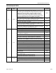
Digital Pins:
Name Type Circuit Description
COM3,
COM2,
COM1,
COM0
O 5
LCD common outputs: These 4 pins provide the select signals for the LCD
display.
SEG0…SEG18 O 5 Dedicated LCD segment output pins.
SEG24/DIO4…
SEG31/DIO11
I/O 3, 4, 5
Multi-use pins, configurable as either LCD SEG driver or DIO. (DIO4 = SCK,
DIO5 = SDA when configured as EEPROM interface, WPULSE = DIO6,
VARPULSE = DIO7 when configured as pulse outputs). If unused, these
pins must be configured as outputs.
SEG34/DIO14…
SEG37/DIO17
I/O 3, 4, 5
Multi-use pins, configurable as either LCD SEG driver or DIO. If unused,
these pins must be configured as outputs.
SEG39/DIO19…
SEG41/DIO21
I/O
3, 4, 5
Multi-use pins, configurable as LCD driver or DIO (QFN 68 package only). If
unused, these pins must be configured as outputs.
E_RXTX/SEG38
E_RST/SEG32
I/O 1, 4, 5
Multi-use pins, configurable as either emulator port pins (when ICE_E pulled
high) or LCD SEG drivers (when ICE_E tied to GND).
E_TCLK/SEG33
O
4, 5
ICE_E I
2
ICE enable. When zero, E_RST, E_TCLK, and E_RXTX become SEG32,
SEG33, and SEG38 respectively. For production units, this pin should be
pulled to GND to disable the emulator port. This pin should be brought out to
the programming interface in order to create a way for reprogramming parts
that have the SECURE bit set.
CKTEST/SEG19 O 4, 5
Multi-use pin, configurable as either Clock PLL output or LCD segment
driver. Can be enabled and disabled by CKOUT_EN.
TMUXOUT O
4
Digital output test multiplexer. Controlled by TMUX[4:0].
OPT_RX/DIO1 I/O
3, 4, 7
Multi-use pin, configurable as Optical Receive Input or general DIO. When
configured as OPT_RX, this pin receives a signal from an external photo-
detector used in an IR serial interface. If unused, this pin must be
configured as an output or terminated to V3P3D or GNDD.
OPT_TX/DIO2 I/O
3, 4
Multi-use pin, configurable as Optical LED Transmit Output, WPULSE,
RPULSE, or general DIO. When configured as OPT_TX, this pin is capable
of directly driving an LED for transmitting data in an IR serial interface. If
unused, this pin must be configured as an output or terminated to
V3P3D or GNDD.
DIO3 I/O
3, 4
DIO pin (QFN 68 package only)
RESET I
3
This input pin resets the chip into a known state. For normal operation, this
pin is connected to GNDD. To reset the chip, this pin should be pulled high.
No external reset circuitry is necessary.
RX I 3
UART input. If unused, this pin must be terminated to V3P3D or GNDD.
TX O
4
UART output.
TEST I
7
Enables Production Test. Must be grounded in normal operation.
PB I
3
Push button input. A rising edge sets the IE_PB flag and causes the part to
wake up if it is in SLEEP or LCD mode. PB does not have an internal pull-up
or pull-down. If unused, this pin must be terminated to GNDD.
X4MHZ I
3
This pin must be connected to GNDD.
Pin types: P = Power, O = Output, I = Input, I/O = Input/Output
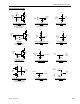
The circuit number denotes the equivalent circuit, as specified on the following page.