
Datasheet

71M6521DE/DH/FE Data Sheet
Rev 3 Page: 49 of 107
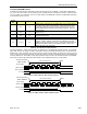
System Timing Summary
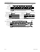
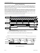
Figure 16 summarizes the timing relationships between the input MUX states, the CE_BUSY signal, and the two
serial output streams. In this example, MUX_DIV=4 and FIR_LEN=1 (384). The duration of each MUX frame is 1 +
MUX_DIV * 2 if FIR_LEN=288, and 1 + MUX_DIV * 3 if FIR_LEN=384. An ADC conversion will always consume an
integer number of CK32 clocks. Followed by the conversions is a single CK32 cycle where the bandgap voltage is
allowed to recover from the change in CROSS.
Each CE program pass begins when ADC0 (channel IA) conversion begins. Depending on the length of the CE
program, it may continue running until the end of the ADC3 (VB) conversion. CE opcodes are constructed to ensure
that all CE code passes consume exactly the same number of cycles. The result of each ADC conversion is inserted
into the CE DRAM when the conversion is complete. The CE code is written to tolerate sudden changes in ADC data.
The exact CK count when each ADC value is loaded into DRAM is shown in Figure 16.
Figure 16 also shows that the serial RTM data stream begins transmitting at the beginning of state ‘S.’ RTM,
consisting of 140 CK cycles, will always finish before the next code pass starts.
Figure 16: Timing Relationship between ADC MUX, Compute Engine, and Serial Transfers.
CKTEST
TMUXOUT/RTM
FLAG
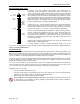
RTM DATA0 (32 bits)
LSB
SIGN
LSB
SIGN
RTM DATA1 (32 bits)
LSB
LSB
SIGN
SIGN
RTM DATA2 (32 bits)
RTM DATA3 (32 bits)
0 1 30 31 0 1 30 31 0 1 30 31 0 1 30 31
FLAG
FLAG
FLAG
MUX_SYNC
CK32
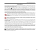
Figure 17: RTM Output Format
CK32
MUX STATE
0
MUX_DIV Conversions, MUX_DIV=1 (4 conversions) is shown
Settle
ADC MUX Frame
ADC EXECUTION
S
MUX_SYNC
S
CE_EXECUTION
RTM
140
MAX CK COUNT
0 450
150
900 1350 1800
ADC0 ADC1 ADC2 ADC3
CK COUNT = CE_CYCLES + floor((CE_CYCLES + 2) / 5)
NOTES:
1. ALL DIMENSIONS ARE 5MHZ CK COUNTS.
2. THE PRECISE FREQUENCY OF CK IS 150*CRYSTAL FREQUENCY = 4.9152MHz.
3. XFER_BUSY OCCURS ONCE EVERY (PRESAMPS * SUM_CYCLES) CODE PASSES.
CE_BUSY
XFER_BUSY
INITIATED BY A CE OPCODE AT END OF SUM INTERVAL
ADC TIMING
CE TIMING
RTM TIMING
1 2 3