
Datasheet
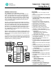
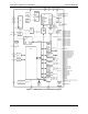
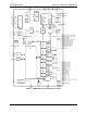
Table Of Contents
- 1 Hardware Description
- 1.1 Hardware Overview
- 1.2 Analog Front End (AFE)
- 1.3 Digital Computation Engine (CE)
- 1.4 80515 MPU Core
- 1.4.1 Memory Organization and Addressing
- 1.4.2 Special Function Registers (SFRs)
- 1.4.3 Generic 80515 Special Function Registers
- 1.4.4 Special Function Registers (SFRs) Specific to the 71M6531D/F and 71M6532D/F
- 1.4.5 Instruction Set
- 1.4.6 UARTs
- 1.4.7 Timers and Counters
- 1.4.8 WD Timer (Software Watchdog Timer)
- 1.4.9 Interrupts
- 1.5 On-Chip Resources
- 1.5.1 Oscillator
- 1.5.2 Internal Clocks
- 1.5.3 Real-Time Clock (RTC)
- 1.5.4 Temperature Sensor
- 1.5.5 Physical Memory
- 1.5.6 Optical Interface
- 1.5.7 Digital I/O – 71M6531D/F
- 1.5.8 Digital I/O – 71M6532D/F
- 1.5.9 Digital IO – Common Characteristics for 71M6531D/F and 71M6532D/F
- 1.5.10 LCD Drivers – 71M6531D/F
- 1.5.11 LCD Drivers – 71M6532D/F
- 1.5.12 LCD Drivers – Common Characteristics for 71M6531D/F and 71M6532D/F
- 1.5.13 Battery Monitor
- 1.5.14 EEPROM Interface
- 1.5.15 SPI Slave Port
- 1.5.16 Hardware Watchdog Timer
- 1.5.17 Test Ports (TMUXOUT pin)
- 2 Functional Description
- 3 Application Information
- 3.1 Connection of Sensors
- 3.2 Connecting 5-V Devices
- 3.3 Temperature Measurement
- 3.4 Temperature Compensation
- 3.5 Connecting LCDs
- 3.6 Connecting I2C EEPROMs
- 3.7 Connecting Three-Wire EEPROMs
- 3.8 UART0 (TX/RX)
- 3.9 Optical Interface (UART1)
- 3.10 Connecting the V1 Pin
- 3.11 Connecting the Reset Pin
- 3.12 Connecting the Emulator Port Pins
- 3.13 Connecting a Battery
- 3.14 Flash Programming
- 3.15 MPU Firmware
- 3.16 Crystal Oscillator
- 3.17 Meter Calibration
- 4 Firmware Interface
- 4.1 I/O RAM and SFR Map – Functional Order
- 4.2 I/O RAM Description – Alphabetical Order
- 4.3 CE Interface Description
- 5 Electrical Specifications
- 5.1 Absolute Maximum Ratings
- 5.2 Recommended External Components
- 5.3 Recommended Operating Conditions
- 5.4 Performance Specifications
- 5.4.1 Input Logic Levels
- 5.4.2 Output Logic Levels
- 5.4.3 Power-Fault Comparator
- 5.4.4 Battery Monitor
- 5.4.5 Supply Current
- 5.4.6 V3P3D Switch
- 5.4.7 2.5 V Voltage Regulator
- 5.4.8 Low-Power Voltage Regulator
- 5.4.9 Crystal Oscillator
- 5.4.10 LCD DAC
- 5.4.11 LCD Drivers
- 5.4.12 Optical Interface
- 5.4.13 Temperature Sensor
- 5.4.14 VREF
- 5.4.15 ADC Converter, V3P3A Referenced
- 5.5 Timing Specifications
- 5.6 Typical Performance Data
- 5.7 71M6531D/F Package
- 5.8 71M6532D/F Package
- 5.9 Pin Descriptions
- 6 Ordering Information
- 7 Related Information
- 8 Contact Information
- Appendix A: Acronyms
- Appendix B: Revision History

Data Sheet 71M6531D/F-71M6532D/F FDS 6531/6532 005
10 Rev 2
1 Hardware Description
1.1 Hardware Overview
The 71M6531D/F and 71M6532D/F single-chip energy meters integrates all primary functional blocks
required to implement a solid-state electricity meter. Included on the chips are:
• An analog front end (AFE)
• An Independent digital computation engine (CE)
• An 8051-compatible microprocessor (MPU) which executes one instruction per clock cycle (80515)
• A voltage reference
• A temperature sensor
• LCD drivers
• RAM and Flash memory
• A real time clock (RTC)
• A variety of I/O pins
Various current sensor technologies are supported including Current Transformers (CT), Resistive Shunts
and Rogowski coils.
In a typical application, the 32-bit compute engine (CE) of the 71M6531D/F and 71M6532D/F sequentially
process the samples from the voltage inputs on pins IA, VA, IB, VB and performs calculations to measure
active energy (Wh) and reactive energy (VARh), as well as A
2
h and V
2
h for four-quadrant metering.
These measurements are then accessed by the MPU, processed further and output using the peripheral
devices available to the MPU.
In addition to advanced measurement functions, the real time clock function allows the 71M6531D/F and
71M6532D/F to record time of use (TOU) metering information for multi-rate applications and to time-stamp
tamper events. Measurements can be displayed on 3.3 V LCDs commonly used in low-temperature
environments. Flexible mapping of LCD display segments facilitate integration of existing custom LCDs.
Design trade-off between the number of LCD segments and DIO pins can be implemented in software to
accommodate various requirements.
In addition to the temperature-trimmed ultra-precision voltage reference, the on-chip digital temperature
compensation mechanism includes a temperature sensor and associated controls for correction of unwanted
temperature effects on measurement and RTC accuracy, e.g. to meet the requirements of ANSI and IEC
standards. Temperature-dependent external components such as a crystal oscillator, current transformers
(CTs) and their corresponding signal conditioning circuits can be characterized and their correction factors
can be programmed to produce electricity meters with exceptional accuracy over the industrial temperature
range.
One of the two internal UARTs is adapted to support an Infrared LED with internal drive and sense
configuration and can also function as a standard UART. The optical output can be modulated at 38 kHz.
This flexibility makes it possible to implement AMR meters with an IR interface. A block diagram of the
71M6531D/F IC is shown in Figure 1. A block diagram of the 71M6532D/F IC is shown in Figure 2.
1.2 Analog Front End (AFE)
The AFE consists of an input multiplexer, a delta-sigma A/D converter and a voltage reference.
1.2.1 Signal Input Pins
All analog signal input pins are sensitive to voltage. In the 71M6531D/F, the VA and VB pins, as well as the
IA and IB pins are single-ended. In the 71M6532D/F, the IAP/IAN and IBP/IBN pins can be programmed
individually to be differential (see I/O RAM bit SEL_IAN and SEL_IBN) or single-ended. The differential signal
is applied between the IAP and IAN input pins and between the IBP and IBN input pins. Single-ended
signals are applied to the IAP and IBP input pins whereas the common signal, return, is the V3P3A pin.
When using the differential mode, inputs can be chopped, i.e. a connection from V3P3A to IAP or IAN (or
IBP an IBN, respectively) alternates in each multiplexer cycle.