
Datasheet
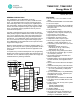
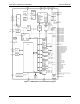
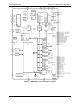
Table Of Contents
- 1 Hardware Description
- 1.1 Hardware Overview
- 1.2 Analog Front End (AFE)
- 1.3 Digital Computation Engine (CE)
- 1.4 80515 MPU Core
- 1.4.1 Memory Organization and Addressing
- 1.4.2 Special Function Registers (SFRs)
- 1.4.3 Generic 80515 Special Function Registers
- 1.4.4 Special Function Registers (SFRs) Specific to the 71M6531D/F and 71M6532D/F
- 1.4.5 Instruction Set
- 1.4.6 UARTs
- 1.4.7 Timers and Counters
- 1.4.8 WD Timer (Software Watchdog Timer)
- 1.4.9 Interrupts
- 1.5 On-Chip Resources
- 1.5.1 Oscillator
- 1.5.2 Internal Clocks
- 1.5.3 Real-Time Clock (RTC)
- 1.5.4 Temperature Sensor
- 1.5.5 Physical Memory
- 1.5.6 Optical Interface
- 1.5.7 Digital I/O – 71M6531D/F
- 1.5.8 Digital I/O – 71M6532D/F
- 1.5.9 Digital IO – Common Characteristics for 71M6531D/F and 71M6532D/F
- 1.5.10 LCD Drivers – 71M6531D/F
- 1.5.11 LCD Drivers – 71M6532D/F
- 1.5.12 LCD Drivers – Common Characteristics for 71M6531D/F and 71M6532D/F
- 1.5.13 Battery Monitor
- 1.5.14 EEPROM Interface
- 1.5.15 SPI Slave Port
- 1.5.16 Hardware Watchdog Timer
- 1.5.17 Test Ports (TMUXOUT pin)
- 2 Functional Description
- 3 Application Information
- 3.1 Connection of Sensors
- 3.2 Connecting 5-V Devices
- 3.3 Temperature Measurement
- 3.4 Temperature Compensation
- 3.5 Connecting LCDs
- 3.6 Connecting I2C EEPROMs
- 3.7 Connecting Three-Wire EEPROMs
- 3.8 UART0 (TX/RX)
- 3.9 Optical Interface (UART1)
- 3.10 Connecting the V1 Pin
- 3.11 Connecting the Reset Pin
- 3.12 Connecting the Emulator Port Pins
- 3.13 Connecting a Battery
- 3.14 Flash Programming
- 3.15 MPU Firmware
- 3.16 Crystal Oscillator
- 3.17 Meter Calibration
- 4 Firmware Interface
- 4.1 I/O RAM and SFR Map – Functional Order
- 4.2 I/O RAM Description – Alphabetical Order
- 4.3 CE Interface Description
- 5 Electrical Specifications
- 5.1 Absolute Maximum Ratings
- 5.2 Recommended External Components
- 5.3 Recommended Operating Conditions
- 5.4 Performance Specifications
- 5.4.1 Input Logic Levels
- 5.4.2 Output Logic Levels
- 5.4.3 Power-Fault Comparator
- 5.4.4 Battery Monitor
- 5.4.5 Supply Current
- 5.4.6 V3P3D Switch
- 5.4.7 2.5 V Voltage Regulator
- 5.4.8 Low-Power Voltage Regulator
- 5.4.9 Crystal Oscillator
- 5.4.10 LCD DAC
- 5.4.11 LCD Drivers
- 5.4.12 Optical Interface
- 5.4.13 Temperature Sensor
- 5.4.14 VREF
- 5.4.15 ADC Converter, V3P3A Referenced
- 5.5 Timing Specifications
- 5.6 Typical Performance Data
- 5.7 71M6531D/F Package
- 5.8 71M6532D/F Package
- 5.9 Pin Descriptions
- 6 Ordering Information
- 7 Related Information
- 8 Contact Information
- Appendix A: Acronyms
- Appendix B: Revision History

Data Sheet 71M6531D/F-71M6532D/F FDS 6531/6532 005
2 Rev 2
Table of Contents
1 Hardware Description ....................................................................................................................... 10
1.1 Hardware Overview ................................................................................................................... 10
1.2 Analog Front End (AFE) ............................................................................................................. 10
1.2.1 Signal Input Pins ............................................................................................................ 10
1.2.2 Input Multiplexer............................................................................................................. 11
1.2.3 A/D Converter (ADC) ..................................................................................................... 12
1.2.4 FIR Filter ........................................................................................................................ 12
1.2.5 Voltage References ....................................................................................................... 12
1.2.6 Temperature Sensor ...................................................................................................... 14
1.2.7 Battery Monitor............................................................................................................... 14
1.2.8 AFE Functional Description ........................................................................................... 14
1.2.9 Digital Computation Engine (CE) ................................................................................... 15
1.2.10 Meter Equations ............................................................................................................. 16
1.2.11 Real-Time Monitor ......................................................................................................... 16
1.2.12 Pulse Generators ........................................................................................................... 16
1.2.13 Data RAM (XRAM) ........................................................................................................ 17
1.2.14 Delay Compensation ..................................................................................................... 17
1.2.15 CE Functional Overview ................................................................................................ 17
1.3 80515 MPU Core ....................................................................................................................... 19
1.3.1 Memory Organization and Addressing .......................................................................... 19
1.3.2 Special Function Registers (SFRs)................................................................................ 21
1.3.3 Generic 80515 Special Function Registers ................................................................... 22
1.3.4 Special Function Registers (SFRs) Specific to the 71M6531D/F and 71M6532D/F ..... 24
1.3.5 Instruction Set ................................................................................................................ 26
1.3.6 UARTs ........................................................................................................................... 26
1.3.7 Timers and Counters ..................................................................................................... 28
1.3.8 WD Timer (Software Watchdog Timer) ......................................................................... 30
1.3.9 Interrupts ........................................................................................................................ 30
1.4 On-Chip Resources ................................................................................................................... 36
1.4.1 Oscillator ........................................................................................................................ 36
1.4.2 Internal Clocks ............................................................................................................... 36
1.4.3 Real-Time Clock (RTC) ................................................................................................. 37
1.4.4 Temperature Sensor ...................................................................................................... 38
1.4.5 Physical Memory............................................................................................................ 38
1.4.6 Optical Interface ............................................................................................................. 40
1.4.7 Digital I/O – 71M6531D/F .............................................................................................. 41
1.4.8 Digital I/O – 71M6532D/F .............................................................................................. 43
1.4.9 Digital IO – Common Characteristics for 71M6531D/F and 71M6532D/F .................... 44
1.4.10 LCD Drivers – 71M6531D/F .......................................................................................... 45
1.4.11 LCD Drivers – 71M6532D/F .......................................................................................... 46
1.4.12 LCD Drivers – Common Characteristics for 71M6531D/F and 71M6532D/F ............... 46
1.4.13 Battery Monitor............................................................................................................... 46
1.4.14 EEPROM Interface ........................................................................................................ 46
1.4.15 SPI Slave Port................................................................................................................ 49
1.4.16 Hardware Watchdog Timer ............................................................................................ 52
1.4.17 Test Ports (TMUXOUT pin) ........................................................................................... 53