
Datasheet
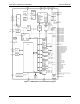
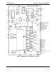
Table Of Contents
- 1 Hardware Description
- 1.1 Hardware Overview
- 1.2 Analog Front End (AFE)
- 1.3 Digital Computation Engine (CE)
- 1.4 80515 MPU Core
- 1.4.1 Memory Organization and Addressing
- 1.4.2 Special Function Registers (SFRs)
- 1.4.3 Generic 80515 Special Function Registers
- 1.4.4 Special Function Registers (SFRs) Specific to the 71M6531D/F and 71M6532D/F
- 1.4.5 Instruction Set
- 1.4.6 UARTs
- 1.4.7 Timers and Counters
- 1.4.8 WD Timer (Software Watchdog Timer)
- 1.4.9 Interrupts
- 1.5 On-Chip Resources
- 1.5.1 Oscillator
- 1.5.2 Internal Clocks
- 1.5.3 Real-Time Clock (RTC)
- 1.5.4 Temperature Sensor
- 1.5.5 Physical Memory
- 1.5.6 Optical Interface
- 1.5.7 Digital I/O – 71M6531D/F
- 1.5.8 Digital I/O – 71M6532D/F
- 1.5.9 Digital IO – Common Characteristics for 71M6531D/F and 71M6532D/F
- 1.5.10 LCD Drivers – 71M6531D/F
- 1.5.11 LCD Drivers – 71M6532D/F
- 1.5.12 LCD Drivers – Common Characteristics for 71M6531D/F and 71M6532D/F
- 1.5.13 Battery Monitor
- 1.5.14 EEPROM Interface
- 1.5.15 SPI Slave Port
- 1.5.16 Hardware Watchdog Timer
- 1.5.17 Test Ports (TMUXOUT pin)
- 2 Functional Description
- 3 Application Information
- 3.1 Connection of Sensors
- 3.2 Connecting 5-V Devices
- 3.3 Temperature Measurement
- 3.4 Temperature Compensation
- 3.5 Connecting LCDs
- 3.6 Connecting I2C EEPROMs
- 3.7 Connecting Three-Wire EEPROMs
- 3.8 UART0 (TX/RX)
- 3.9 Optical Interface (UART1)
- 3.10 Connecting the V1 Pin
- 3.11 Connecting the Reset Pin
- 3.12 Connecting the Emulator Port Pins
- 3.13 Connecting a Battery
- 3.14 Flash Programming
- 3.15 MPU Firmware
- 3.16 Crystal Oscillator
- 3.17 Meter Calibration
- 4 Firmware Interface
- 4.1 I/O RAM and SFR Map – Functional Order
- 4.2 I/O RAM Description – Alphabetical Order
- 4.3 CE Interface Description
- 5 Electrical Specifications
- 5.1 Absolute Maximum Ratings
- 5.2 Recommended External Components
- 5.3 Recommended Operating Conditions
- 5.4 Performance Specifications
- 5.4.1 Input Logic Levels
- 5.4.2 Output Logic Levels
- 5.4.3 Power-Fault Comparator
- 5.4.4 Battery Monitor
- 5.4.5 Supply Current
- 5.4.6 V3P3D Switch
- 5.4.7 2.5 V Voltage Regulator
- 5.4.8 Low-Power Voltage Regulator
- 5.4.9 Crystal Oscillator
- 5.4.10 LCD DAC
- 5.4.11 LCD Drivers
- 5.4.12 Optical Interface
- 5.4.13 Temperature Sensor
- 5.4.14 VREF
- 5.4.15 ADC Converter, V3P3A Referenced
- 5.5 Timing Specifications
- 5.6 Typical Performance Data
- 5.7 71M6531D/F Package
- 5.8 71M6532D/F Package
- 5.9 Pin Descriptions
- 6 Ordering Information
- 7 Related Information
- 8 Contact Information
- Appendix A: Acronyms
- Appendix B: Revision History

FDS 6531/6532 005 Data Sheet 71M6531D/F-71M6532D/F
Rev 2 5
Figures
Figure 1: 71M6531D/F IC Functional Block Diagram ................................................................................... 8
Figure 2: 71M6532D/F IC Functional Block Diagram ................................................................................... 9
Figure 3: General Topology of a Chopped Amplifier .................................................................................. 13
Figure 4: CROSS Signal with CHOP_E[1:0] = 00 ....................................................................................... 13
Figure 5: AFE Block Diagram (Shown for the 71M6532D/F) ...................................................................... 14
Figure 6: Samples from Multiplexer Cycle .................................................................................................. 18
Figure 7: Accumulation Interval................................................................................................................... 18
Figure 8: Interrupt Structure ........................................................................................................................ 35
Figure 9: Optical Interface ........................................................................................................................... 41
Figure 10: Connecting an External Load to DIO Pins ................................................................................. 45
Figure 11: 3-Wire Interface. Write Command, HiZ=0 ................................................................................ 48
Figure 12: 3-Wire Interface. Write Command, HiZ=1 ................................................................................ 48
Figure 13: 3-Wire Interface. Read Command. ........................................................................................... 49
Figure 14: 3-Wire Interface. Write Command when CNT=0 ...................................................................... 49
Figure 15: 3-Wire Interface. Write Command when HiZ=1 and WFR=1 ................................................... 49
Figure 16: SPI Slave Port: Typical Read and Write operations .................................................................. 51
Figure 17: Functions defined by V1 ............................................................................................................ 52
Figure 18: Voltage, Current, Momentary and Accumulated Energy ........................................................... 54
Figure 19: Timing Relationship between ADC MUX, Compute Engine ...................................................... 55
Figure 20: RTM Output Format ................................................................................................................... 55
Figure 21: Operation Modes State Diagram ............................................................................................... 56
Figure 22: Transition from BROWNOUT to MISSION Mode when System Power Returns ...................... 59
Figure 23: Power-Up Timing with V3P3SYS and VBAT tied together ........................................................ 59
Figure 24: Power-Up Timing with VBAT only.............................................................................................. 60
Figure 25: Wake Up Timing ........................................................................................................................ 61
Figure 26: MPU/CE Data Flow .................................................................................................................... 62
Figure 27: MPU/CE Communication ........................................................................................................... 62
Figure 28: Resistive Voltage Divider ........................................................................................................... 63
Figure 29: CT with Single Ended (Left) and Differential Input (Right) Connection ..................................... 63
Figure 30: Resistive Shunt (Left) and Rogowski Sensor (Right) Connection ............................................. 63
Figure 31: Connecting LCDs ....................................................................................................................... 66
Figure 32: I
2
C EEPROM Connection .......................................................................................................... 66
Figure 33: Three-Wire EEPROM Connection ............................................................................................. 67
Figure 34: Connections for UART0 ............................................................................................................. 67
Figure 35: Connection for Optical Components .......................................................................................... 68
Figure 36: Voltage Divider for V1 ................................................................................................................ 68
Figure 37: External Components for the RESET Pin: Push-button (Left), Production Circuit (Right) ........ 69
Figure 38: External Components for the Emulator Interface ...................................................................... 69
Figure 39: Connecting a Battery ................................................................................................................. 70
Figure 40: CE Data Flow: Multiplexer and ADC.......................................................................................... 96
Figure 41: CE Data Flow: Scaling, Gain Control, Intermediate Variables .................................................. 96
Figure 42: CE Data Flow: Squaring and Summation Stages ...................................................................... 97
Figure 43: SPI Slave Port (MISSION Mode) Timing ................................................................................. 107
Figure 44: Wh Accuracy, 0.1 A to 200 A at 240 V/50 Hz and Room Temperature .................................. 108
Figure 45: QFN-68 Package Outline, Top and Side View ........................................................................ 109
Figure 46: QFN-68 Package Outline, Bottom View .................................................................................. 109
Figure 47: Pinout for QFN-68 Package ..................................................................................................... 110
Figure 48: PCB Land Pattern for QFN 68 Package .................................................................................. 111
Figure 49: PCB Land Pattern for LQFP-100 Package .............................................................................. 112
Figure 50: LQFP-100 Package, Mechanical Drawing ............................................................................... 113
Figure 51: I/O Equivalent Circuits ............................................................................................................. 116