
Datasheet


FDS_6533_6534_004 71M6533/G/H and 71M6534/H Data Sheet
Rev 2 25
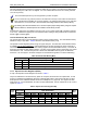
Table 13: Stretch Memory Cycle Width
CKCON[2:0]
Stretch
Value
Read Signal Width
Write Signal Width
memaddr
memrd
memaddr
memwr
000
0
1
1
2
1
001
1
2
2
3
1
010
2
3
3
4
2
011
3
4
4
5
3
100
4
5
5
6
4
101
5
6
6
7
5
110
6
7
7
8
6
111
7
8
8
9
7
1.4.4 71M6533/71M6534-Specific Special Function Registers
Table 14 shows the location and description of the 71M6533/71M6534-specific SFRs.
Table 14: 71M6533/71M6534 Specific SFRs
Register
(Alternate Name)
SFR
Address
Bit Field
Name
R/W Description
EEDATA
0x9E
R/W
I
2
C EEPROM interface data register.
EECTRL
0x9F
R/W
I
2
C EEPROM interface control register.
See Section 1.5.10 EEPROM Interface for a
description of the command and status bits
available for
EECTRL
.
ERASE
(FLSH_ERASE)
0x94
W
This register is used to initiate either the Flash
Mass Erase cycle or the Flash Page Erase cycle.
See the Flash Memory section for details.
FL_BANK[2:0]
0xB6[2:0]
R/W
Flash Bank Selection.
PGADDR
(FLSH_PGADR)
0xB7
R/W
Flash Page Erase Address register. Contains
the flash memory page address (page 0
through page 127) that will be erased
during the
Page Erase cycle (default = 0x00). Must be re-
written for each new Page Erase cycle.
FLSHCRL
0xB2[0]
FLSH_PWE
R/W
Program Write Enable:
0:
MOVX commands refer to XRAM Space,
normal operation (default).
1: MOVX @DPTR,A moves A to Program
Space (Flash) @ DPTR.
0xB2[1]
FLSH_MEEN
W
Mass Erase Enable:
0: Mass Erase disabled (default).
1: Mass Erase enabled.
Must be re-written for each new Mass Erase cycle.
0xB2[4]
WRPROT_CE*
Protects flash from address CE_LCTN *1024 to
the end of memory from flash page erase.
0xB2[5]
WRPROT_BT*
Protects flash from address 0 to address
BOOT_SIZE*1024 from flash page erase.
0xB2[6]
SECURE
R/W
Enables security provisions that prevent external
reading of flash memory and CE program RAM.
This bit is reset on chip reset and may only be set.
Attempts to write zero are ignored.
0xB2[7]
PREBOOT
R
Indicates that the preboot sequence is active.
* The WRPROT_CE and WRPROT_BT bits can only be cleared when the SECURE bit
is not set. When SECURE = 1, WRPROT_CE and WRPROT_BT can only be set to 1.
A hardware reset is required to clear these bits if SECURE = 1.