
Datasheet
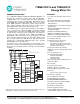

71M6541D/F/G and 71M6542F/G Data Sheet
2 Rev 4
Table of Contents
1 Introduction ....................................................................................................................................... 10
2 Hardware Description ....................................................................................................................... 11
2.1 Hardware Overview ................................................................................................................... 11
2.2 Analog Front End (AFE) ............................................................................................................. 12
2.2.1 Signal Input Pins ............................................................................................................ 14
2.2.2 Input Multiplexer ............................................................................................................ 15
2.2.3 Delay Compensation ..................................................................................................... 19
2.2.4 ADC Pre-Amplifier ......................................................................................................... 20
2.2.5 A/D Converter (ADC) ..................................................................................................... 20
2.2.6 FIR Filter ........................................................................................................................ 20
2.2.7 Voltage References ....................................................................................................... 20
2.2.8 71M6x01 Isolated Sensor Interface (Remote Sensor Interface) ................................... 22
2.3 Digital Computation Engine (CE) ............................................................................................... 24
2.3.1 CE Program Memory ..................................................................................................... 24
2.3.2 CE Data Memory ........................................................................................................... 24
2.3.3 CE Communication with the MPU ................................................................................. 25
2.3.4 Meter Equations ............................................................................................................. 25
2.3.5 Real-Time Monitor (RTM) .............................................................................................. 25
2.3.6 Pulse Generators ........................................................................................................... 27
2.3.7 CE Functional Overview ................................................................................................ 28
2.4 80515 MPU Core ....................................................................................................................... 31
2.4.1 Memory Organization and Addressing .......................................................................... 31
2.4.2 Special Function Registers (SFRs) ............................................................................... 33
2.4.3 Generic 80515 Special Function Registers ................................................................... 34
2.4.4 Instruction Set ................................................................................................................ 37
2.4.5 UARTs ........................................................................................................................... 37
2.4.6 Timers and Counters ..................................................................................................... 39
2.4.7 WD Timer (Software Watchdog Timer) ......................................................................... 41
2.4.8 Interrupts ........................................................................................................................ 41
2.5 On-Chip Resources ................................................................................................................... 48
2.5.1 Physical Memory............................................................................................................ 48
2.5.2 Oscillator ........................................................................................................................ 50
2.5.3 PLL and Internal Clocks ................................................................................................. 50
2.5.4 Real-Time Clock (RTC) ................................................................................................. 51
2.5.5 71M654x Temperature Sensor ...................................................................................... 56
2.5.6 71M654x Battery Monitor ............................................................................................... 57
2.5.7 UART and Optical Interface ........................................................................................... 58
2.5.8 Digital I/O and LCD Segment Drivers ............................................................................ 59
2.5.9 EEPROM Interface ........................................................................................................ 70
2.5.10 SPI Slave Port................................................................................................................ 73
2.5.11 Hardware Watchdog Timer ............................................................................................ 78
2.5.12 Test Ports (TMUXOUT and TMUX2OUT Pins) ............................................................. 78
3 Functional Description ..................................................................................................................... 80
3.1 Theory of Operation ................................................................................................................... 80
3.2 Battery Modes ............................................................................................................................ 81
3.2.1 BRN Mode ..................................................................................................................... 83
3.2.2 LCD Mode ...................................................................................................................... 83
3.2.3 SLP Mode ...................................................................................................................... 84