
Datasheet

71M6541D/F/G and 71M6542F/G Data Sheet
Rev 4
Figures
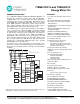
Figure 1: IC Functional Block Diagram ......................................................................................................... 9
Figure 2. 71M6541D/F/G AFE Block Diagram (Local Sensors) ................................................................. 12
Figure 3. 71M6541D/F/G AFE Block Diagram with 71M6x01 .................................................................... 13
Figure 4. 71M6542F/G AFE Block Diagram (Local Sensors) ..................................................................... 13
Figure 5. 71M6542F/G AFE Block Diagram with 71M6x01 ........................................................................ 14
Figure 6: States in a Multiplexer Frame (MUX_DIV[3:0] = 3) ..................................................................... 17
Figure 7: States in a Multiplexer Frame (MUX_DIV[3:0] = 4) ..................................................................... 17
Figure 8: General Topology of a Chopped Amplifier .................................................................................. 21
Figure 9: CROSS Signal with CHOP_E = 00 ............................................................................................... 21
Figure 10: RTM Timing ............................................................................................................................... 26
Figure 11: Timing Relationship Between ADC MUX, CE, and RTM Serial Transfer .................................. 26
Figure 12. Pulse Generator FIFO Timing .................................................................................................... 28
Figure 13: Accumulation Interval ................................................................................................................ 29
Figure 14: Samples from Multiplexer Cycle (MUX_DIV[3:0] = 3) ............................................................... 30
Figure 15: Samples from Multiplexer Cycle (MUX_DIV[3:0] = 4) ............................................................... 30
Figure 16: Interrupt Structure ...................................................................................................................... 47
Figure 17: Automatic Temperature Compensation ..................................................................................... 54
Figure 18: Optical Interface ......................................................................................................................... 58
Figure 19: Optical Interface (UART1) ......................................................................................................... 59
Figure 20: Connecting an External Load to DIO Pins ................................................................................. 60
Figure 21: LCD Waveforms ......................................................................................................................... 68
Figure 22: 3-Wire Interface. Write Command, HiZ=0. ............................................................................... 72
Figure 23: 3-Wire Interface. Write Command, HiZ=1 ................................................................................ 72
Figure 24: 3-Wire Interface. Read Command. ........................................................................................... 72
Figure 25: 3-Wire Interface. Write Command when CNT=0 ...................................................................... 73
Figure 26: 3-Wire Interface. Write Command when HiZ=1 and WFR=1. .................................................. 73
Figure 27: SPI Slave Port - Typical Multi-Byte Read and Write Operations ............................................... 75
Figure 28: Voltage, Current, Momentary and Accumulated Energy ........................................................... 80
Figure 29: Operation Modes State Diagram ............................................................................................... 81
Figure 30: MPU/CE Data Flow .................................................................................................................... 91
Figure 31: Resistive Voltage Divider (Voltage Sensing) ............................................................................. 92
Figure 32. CT with Single-Ended Input Connection (Current Sensing) ...................................................... 92
Figure 33: CT with Differential Input Connection (Current Sensing) .......................................................... 92
Figure 34: Differential Resistive Shunt Connections (Current Sensing) ..................................................... 92
Figure 35. 71M6541D/F/G with Local Sensors ........................................................................................... 93
Figure 36: 71M6541D/F/G with 71M6x01 isolated Sensor ......................................................................... 94
Figure 37: 71M6542F/G with Local Sensors ............................................................................................... 95
Figure 38: 71M6542F/G with 71M6x01 Isolated Sensor ............................................................................ 96
Figure 39: I
2
C EEPROM Connection ........................................................................................................ 100
Figure 40: Connections for UART0 ........................................................................................................... 101
Figure 41: Connection for Optical Components ........................................................................................ 102
Figure 42: External Components for the RESET Pin: Push-Button (Left), Production Circuit (Right) ......... 102
Figure 43: External Components for the Emulator Interface .................................................................... 103
Figure 44: CE Data Flow: Multiplexer and ADC........................................................................................ 137
Figure 45: CE Data Flow: Scaling, Gain Control, Intermediate Variables ................................................ 137
Figure 46: CE Data Flow: Squaring and Summation Stages .................................................................... 138
Figure 47: 64-pin LQFP Package Outline ................................................................................................. 154
Figure 48: 100-pin LQFP Package Outline ............................................................................................... 155
Figure 49. Package Markings (Examples) ................................................................................................ 156
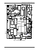
Figure 50: Pinout for the 71M6541D/F/G (LQFP-64 Package) ................................................................. 157
Figure 51: Pinout for the 71M6542F/G (LQFP-100 Package) .................................................................. 158
Figure 52: I/O Equivalent Circuits ............................................................................................................. 163