
Datasheet


71M6543F/71M6543G Data Sheet
v2 5
Figures
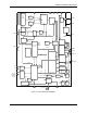
Figure 1: IC Functional Block Diagram ......................................................................................................... 9
Figure 2: AFE Block Diagram (Shunts: One-Local, Three-Remotes) ......................................................... 12
Figure 3. AFE Block Diagram (Four CTs) ................................................................................................... 13
Figure 4: States in a Multiplexer Frame (MUX_DIV[3:0] = 6) ..................................................................... 17
Figure 5: States in a Multiplexer Frame (MUX_DIV[3:0] = 7) ..................................................................... 17
Figure 6: General Topology of a Chopped Amplifier .................................................................................. 21
Figure 7: CROSS Signal with CHOP_E = 00 ............................................................................................... 21
Figure 8: RTM Timing ................................................................................................................................. 26
Figure 9. Pulse Generator FIFO Timing ...................................................................................................... 28
Figure 10: Samples from Multiplexer Cycle (Frame) .................................................................................. 29
Figure 11: Accumulation Interval ................................................................................................................ 29
Figure 12: Interrupt Structure ...................................................................................................................... 45
Figure 13: Automatic Temperature Compensation ..................................................................................... 52
Figure 14: Optical Interface ......................................................................................................................... 57
Figure 15: Optical Interface (UART1) ......................................................................................................... 57
Figure 16: Connecting an External Load to DIO Pins ................................................................................. 59
Figure 17: LCD Waveforms......................................................................................................................... 64
Figure 18: 3-wire Interface. Write Command, HiZ=0. ................................................................................ 66
Figure 19: 3-wire Interface. Write Command, HiZ=1 ................................................................................. 67
Figure 20: 3-wire Interface. Read Command. ............................................................................................ 67
Figure 21: 3-Wire Interface. Write Command when CNT=0 ...................................................................... 67
Figure 22: 3-wire Interface. Write Command when HiZ=1 and WFR=1. ................................................... 67
Figure 23: SPI Slave Port - Typical Multi-Byte Read and Write operations ................................................ 69
Figure 24: Voltage, Current, Momentary and Accumulated Energy ........................................................... 74
Figure 25: Operation Modes State Diagram ............................................................................................... 75
Figure 26: MPU/CE Data Flow .................................................................................................................... 84
Figure 27: Resistive Voltage Divider (Voltage Sensing) ............................................................................. 85
Figure 28. CT with Single-Ended Input Connection (Current Sensing) ...................................................... 85
Figure 29: CT with Differential Input Connection (Current Sensing) .......................................................... 85
Figure 30: Differential Resistive Shunt Connections (Current Sensing) ..................................................... 85
Figure 31: System Using Three-Remotes and One-Local (Neutral) Sensor .............................................. 86
Figure 32. System Using Current Transformers ......................................................................................... 87
Figure 33: I
2
C EEPROM Connection .......................................................................................................... 92
Figure 34: Connections for UART0 ............................................................................................................. 92
Figure 35: Connection for Optical Components .......................................................................................... 93
Figure 36: External Components for the RESET Pin: Push-Button (Left), Production Circuit (Right) ........ 94
Figure 37: External Components for the Emulator Interface ...................................................................... 94
Figure 38: CE Data Flow: Multiplexer and ADC........................................................................................ 128
Figure 39: CE Data Flow: Scaling, Gain Control, Intermediate Variables for one Phase ......................... 128
Figure 40: CE Data Flow: Squaring and Summation Stages .................................................................... 129
Figure 41: 100-pin LQFP Package Outline ............................................................................................... 145
Figure 42: Pinout for the LQFP-100 Package ........................................................................................... 146
Figure 43: I/O Equivalent Circuits ............................................................................................................. 151