
Manual

UG_1x22_052 73M1822/73M1922 Implementer’s Guide
Rev. 1.0 7
3.1.3 MAFE Interface Configuration
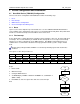
R/W
ADDR
07
06
05
04
03
02
01
00
Write 0x01 DYSEN NSLAVE[2:0] MSIDEN MSID SCK32
Write 0x02 TMEN ENLPW SPOS HC
The MAFE interface must be properly configured by the user before the user can properly access the
device. The device is powered up out of reset in a default state that may not match the final desired
MAFE interface operating mode. The user must be able to operate in this default mode out of reset to
configure the MAFE interface registers for proper long term stable operation. Refer to the
73M1822/73M1922 Data Sheet (Section 8) for instructions on configuring the MAFE interface for optimal
operation.
3.1.4 Clock and Sample Rate Management
The clock and sample rate are managed through a series of registers in the host side device. Refer to
the 73M1822/73M1922 Data Sheet (Section 7) for instructions on configuring the device registers for
optimal operation in various clock and sample rates. Please note the Barrier and PLL can be expected to
temporarily become out of Sync and Lock respectively during a Clock or Sample Rate change. Please
note that, unlike and barrier sync loss due to an error condition, the user can assume the line side
registers will preserve their contents during a sample rate change
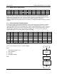
R/W
ADDR
07
06
05
04
03
02
01
00
RW 0x08 PSEQ7 PSEQ6 PSEQ5 PSEQ4 PSEQ3 PSEQ2 PSEQ1 PSEQ0
RW 0x09 PRST2 PRST1 PRST0 PDVSR4 PDVSR3 PDVSR2 PDVSR1 PDVSR0
RW 0x0A ICHP3 ICHP2 ICHP1 ICHP0 Reserved KVCOH2 KVCOH1 KVCOH0
RW 0x0B Reserved NDVSR6 NDVSR5 NDVSR4 NDVSR3 NDVSR2 NDVSR1 NDVSR0
RW 0x0C NSEQ7 NSEQ6 NSEQ5 NSEQ4 NSEQ3 NSEQ2 NSEQ1 NSEQ0
RW 0x0D LOKDET SLHS Reserved Reserved CHNGFS NRST2 NRST1 NRST0
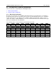
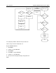
The temporary variables defined in this procedure are:
VAL1 = System appropriate values for RG08 RG0D
Begin
1. Write RG08 RG0D = VAL1.
2. Write CHNGFS = 1
3. Wait 10ms
4. Read RG03, RG0D.
END
Start
Configure
Crystal/PLL
registers
Write CHNGFS
Read
RG03,RG0D
End