
Owner's manual


UG_1x66B_016 73M1866B/73M1966B Implementer’s Guide
Rev. 1.3 9
3.1.4 PCM Interface Configuration
The PCM Highway Interface is described in Section 8 of the 73M1866B/73M1966B Data Sheet. The
PCM Highway Clock and Frame Sync signals must be stable and running at legal values for the
73M1x66B device to operate properly.
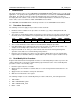
After the device has locked to PCLK and FS the user must configure the PCM interface for the specific
system it resides on. The PCM configuration settings can change per call or remain static over the power
cycle but before setting the PCMEN bit = 1, the user should make sure to set all other PCM register
settings.
The settings that control the PCM Highway interface can be set via the SPI bus without a running PCLK
and FS. The following registers control the PCM Highway interface.
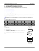
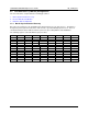
0x20 TPOL TTS6 TTS5 TTS4 TTS3 TTS2 TTS1 TTS0
Write
VAL1
0x21 RPOL RTS6 RTS5 RTS4 RTS3 RTS2 RTS1 RTS0
Write
VAL2
0x22 SR ADJ RCS2 RCS1 RCS0 TCS2 TCS1 TCS0
Write
VAL3
0x23 PCMEN MASTER PCODE3 PCODE2 PCODE1 PCODE0 LIN LAW
Write 0/1 X X X X X
VAL4
The temporary variables defined in this procedure are:
VAL1 = System appropriate value to write to the TPOL and TTS[6:0] bits.
VAL2 = system appropriate value to write to the RPOL and RTS[6:0] bits.
VAL3 = System appropriate value to write to the SR, ADJ, RCS[2:0] and TCS[2:0] bits.
VAL4 = System appropriate value to write to the LIN and LAW bits.
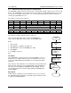
Begin
1. Write PCMEN = 0.
2. Configure other PCM interface registers: Write VAL1 to RG20, VAL2 to RG21,
VAL3 to RG22 and VAL4 to RG23.
3. Write PCMEN = 1.
End
Configure PCM
Interface
PCMEN = 0
RG20 = VAL1
RG21 = VAL2
RG22 = VAL3
RG23 = VAL4
PCMEN = 1
Exit