
Datasheet


73M1903 Data Sheet DS_1903_032
10 Rev. 2.1
2.1 GPIO
The 73M1903 modem AFE device provides 8 user defined I/O pins. Each pin is programmed separately
as either an input or an output by a bit in a direction register. If the bit in the direction register is set high,
the corresponding pin is an input whose value is read from the GPIO data register. If it is low, the pin will
be treated as an output whose value is set by the GPIO data register.
To avoid unwanted current contention and consumption in the system from the GPIO port before the
GPIO is configured after a reset, the GPIO port I/Os are initialized to a high impedance state. The input
structures are protected from floating inputs, and no output levels are driven by any of the GPIO pins.
The GPIO pins are configured as inputs or outputs when the host controller (or DSP) writes to the GPIO
direction register. The GPIO direction and data registers are initialized to all ones (FFh) upon reset.
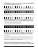
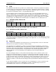
2.1.1 GPIO Data (GPIO): Address 02h
Reset State FFh
Bit 7 Bit 6 Bit 5 Bit 4 Bit 3 Bit 2 Bit 1 Bit 0
GPIO7 GPIO6 GPIO5 GPIO4 GPIO3 GPIO2 GPIO1 GPIO0
Bits in this register will be asserted on the GPIO(7:0) pins if the corresponding direction register bit is a 0.
Reading this address will return data reflecting the values of pins GPIO(7:0).
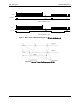
2.1.2 GPIO Direction (DIR): Address 03h
Reset State FFh
Bit 7 Bit 6 Bit 5 Bit 4 Bit 3 Bit 2 Bit 1 Bit 0
DIR7 DIR6 DIR5 DIR4 DIR3 DIR2 DIR1 DIR0
This register is used to designate the GPIO pins as either inputs or outputs. If the register bit is low, the
corresponding GPIO pin is programmed as an output. If the register bit is a 1, the corresponding pin will
be treated as an input.
2.2 Analog I/O
Figure 4 shows the block diagram of the analog front end. The analog interface circuit uses differential
transmit and receive signals to and from the external circuitry.
The hybrid driver in the 73M1903 IC is capable of connecting directly, but not limited to, a transformer-
based Direct Access Arrangement (DAA). The hybrid driver is capable of driving the DAA’s line coupling
transformer, which carries an impedance on the primary side that is typically rated at 600 Ω, depending
on the transformer and matching network. The hybrid drivers can also drive high impedance loads
without modification. The class AB behavior of the amplifiers provides load dependent power
consumption.
An on-chip band gap voltage is used to provide an internal voltage reference and bias currents for the
analog receive and transmit channels. The reference derived from the bandgap, nominally 1.25 Volts, is
multiplied to 1.36 Volts and output at the VREF pin. Several voltage references, nominally 1.25 Volts, are
used in the analog circuits. The band gap and reference circuits are disabled after a chip reset since the
ENFE bit is reset to a default state of zero. When ENFE=0, the band gap voltage and the analog bias
currents are disabled. In this case all of the analog circuits are powered down and draw less than 5 μA of
current.
A clock generator (CKGN) is used to create all of the non-overlapping phase clocks needed for the time
sampled switched-capacitor circuits, ASDM, DAC1, and TLPF. The CKGN input is two times the
analog/digital interface sample rate or 3.072 MHz clock for Fs=8 kHz.