
Datasheet

73M1866B/73M1966B Data Sheet DS_1x66B_001
2 Rev. 1.6
Table of Contents
1 Introduction ................................................................................................................................... 6
2 Pinout ............................................................................................................................................. 8
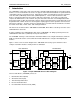
2.1 73M1906B 20-Pin TSSOP Pinout ............................................................................................ 8
2.2 73M1916 20-Pin TSSOP Pinout .............................................................................................. 9
2.3 73M1906B 32-Pin QFN Pinout .............................................................................................. 10
2.4 73M1916 32-Pin QFN Pinout ................................................................................................ 12
2.5 73M1866B Pinout ................................................................................................................. 14
2.6 Requisite Use of Exposed Bottom Pad on 73M1866B and 73M1966B QFN Packages .......... 15
3 Electrical Characteristics and Specifications............................................................................. 16
3.1 Isolation Barrier Characteristics ............................................................................................. 16
3.2 Electrical Specifications......................................................................................................... 16
3.2.1 Absolute Maximum Ratings ....................................................................................... 16
3.2.2 Recommended Operating Conditions ........................................................................ 16
3.2.3 DC Characteristics..................................................................................................... 17
3.3 Interface Timing Specification................................................................................................ 18
3.3.1 SPI Interface ............................................................................................................. 18
3.3.2 PCM Highway Interface ............................................................................................. 19
3.4 Analog Specifications ............................................................................................................ 20
3.4.1 DC Specifications ...................................................................................................... 20
3.4.2 Call Progress Monitor ................................................................................................ 21
3.5 73M1x66B Line-Side Electrical Specifications (73M1916) ...................................................... 22
3.6 Reference and Regulation ..................................................................................................... 23
3.7 DC Transfer Characteristics .................................................................................................. 23
3.8 Transmit Path ....................................................................................................................... 24
3.9 Receive Path ........................................................................................................................ 25
3.10 Transmit Hybrid Cancellation ................................................................................................ 26
3.11 Receive Notch Filter .............................................................................................................. 26
3.12 Detectors .............................................................................................................................. 27
3.12.1 Over-Voltage Detector ............................................................................................... 27
3.12.2 Over-Current Detector ............................................................................................... 27
3.12.3 Under-Voltage Detector ............................................................................................. 27
3.12.4 Over-Load Detector ................................................................................................... 27
4 Applications Information ............................................................................................................. 28
4.1 Example Schematic of the 73M1966B and 73M1866B .......................................................... 28
4.2 Bill of Materials...................................................................................................................... 30
4.3 Over-Voltage and EMI Protection .......................................................................................... 31
4.4 Isolation Barrier Pulse Transformer ....................................................................................... 32
5 SPI Interface ................................................................................................................................. 33
6 Control and Status Registers ...................................................................................................... 37
7 Hardware Control Functions ....................................................................................................... 41
7.1 Device Revision .................................................................................................................... 41
7.2 Interrupt Control .................................................................................................................... 41
7.3 Power Management .............................................................................................................. 42
7.4 Device Clock Management.................................................................................................... 42
7.5 GPIO Registers ..................................................................................................................... 43
7.6 Call Progress Monitor ............................................................................................................ 44
7.7 16 kHz Operation of Call Progress Monitor ............................................................................ 44
7.8 Device Reset ........................................................................................................................ 44
8 PCM Highway Interface and Signal Processing ......................................................................... 45
8.1 PCM Highway Interface Timing ............................................................................................. 45
8.2 PCM Clock Frequencies ........................................................................................................ 47
8.3 Master Mode ......................................................................................................................... 47
8.4 A-law / μ-law Compander ...................................................................................................... 47