
Datasheet

73M1866B/73M1966B Data Sheet DS_1x66B_001
8 Rev. 1.6
2 Pinout
The 73M1906B and the 73M1916 are supplied as 20-pin TSSOP packages and as 32-pin QFN packages.
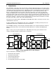
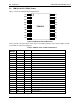
2.1 73M1906B 20-Pin TSSOP Pinout
Figure 2 shows the 73M1906B 20-pin TSSOP pinout.
73M1906B
1
2
3
4
5
6
7
8
9
10 11
12
13
14
15
16
17
18
19
20
CS
VPD
DR
DX
FS
PCLKO
PCLKI
VNA/VND
AOUT
VPA VNT
SCLK
SDI
SDIT
SDO
RST
PRM
PRP
VPT
INT
Figure 2: 73M1906B 20-Pin TSSOP Pinout
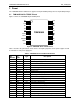
Table 1 describes the pin functions for the device. Decoupling capacitors on the power supplies should
be included for each pair of supply pins.
Table 1: 73M1906B 20-Pin TSSOP Pin Definitions
Pin
Number
Pin
Name
Type Description
1
CS
I SPI chip select (active low)
2 VPD PWRI Positive digital supply
3 DR I PCM transmit data sent to the D to A
4 DX O PCM received data from the A to D
5
FS
I/O PCM frame synchronization
6 PCLKO O PCM clock output
7 PCLKI I PCM clock in
8 VNA/VND GND Negative analog/digital ground
9 AOUT O Audio output – must be buffered for speaker
10 VPA PWRI Positive analog supply
11 VNT GND Negative transformer supply
12 PRM I/O Transformer primary minus
13 PRP I/O Transformer primary plus
14 VPT PWRI Positive transformer supply
15
RST
I Hardware reset (active low)
16 SDIT O SPI data out for daisy chain mode
17 SDI I SPI data in
18 SDO O SPI data out
19
INT
O Interrupt / ring detect (active low – open drain)
20
SCLK
I
SPI clock