
Datasheet

DS_1x66B_001 73M1866B/73M1966B Data Sheet
Rev. 1.6 9
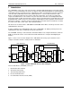
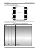
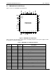
2.2 73M1916 20-Pin TSSOP Pinout
Figure 3 shows the 73M1916 20-pin TSSOP pinout.
73M1916
1
2
3
4
5
6
7
8
9
10 11
12
13
14
15
16
17
18
19
20
DCI
RGN
RGP
OFH
VNX
SCP
MID
VPX
SRE
SRB VBG
DCS
DCD
TXM
RXM
RXP
ACS
VNS
VPS
DCG
Figure 3: 73M1916 20-Pin TSSOP Pinout
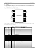
Table 2 describes the pin functions for the device. Decoupling capacitors on the power supplies should
be included for each pair of supply pins.
Table 2: 73M1916 20-Pin TSSOP Pin Definitions
Pin
Number
Pin Name Type Description
1 DCI I DC loop input
2 RGN I Ring detect negative voltage input
3 RGP I Ring detect positive voltage input
4 OFH O Off-hook control
5 VNX GND Negative supply voltage (line side of the barrier)
6 SCP I/O Positive side of the secondary pulse transformer winding
7 MID I/O Charge pump midpoint
8
VPX
PWR
Supply from the barrier
9 SRE I Voltage regulator sense
10 SRB O Voltage regulator drive
11
VBG
O
VBG bypass, connect to 0.1 μF capacitor to VNS
12 ACS I AC current sense
13 VNS GND Analog negative supply voltage
14 VPS PWRO Analog positive supply voltage (output)
15 RXP I Receive plus – signal input
16 RXM I Receive minus – signal input
17 TXM O Transmit minus – transhybrid cancellation output
18 DCD O DC loop output
19 DCS I DC loop current sense
20 DCG O DC loop control