
Datasheet


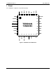


DS_8009C_025 73S8009C Data Sheet
Rev. 1.5 7
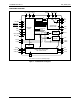
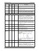
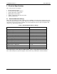
Table 1 describes the pin functions for the device.
Table 1: 73S8009C Pin Definitions
Pin
Name
Pin
(QFN32)
Type
Equivalent
Circuit
Description
Card Interface
I/O 22 IO Figure 16 Card I/O: Data signal to/from card. Includes a pull-up
resistor to V
CC.
AUX1 21 IO Figure 16 AUX1: Auxiliary data signal to/from card. Includes a
pull-up resistor to V
CC.
AUX2 20 IO Figure 16 AUX2: Auxiliary data signal to/from card. Includes a
pull-up resistor to V
CC.
RST 18 O Figure 15 Card reset: provides reset (RST) signal to card. RST is
the pass through signal on RSTIN. Internal control logic
will hold RST low when card is not activated or VCC is
too low.
CLK 16 O Figure 14 Card clock: provides clock signal (CLK) to card. CLK is
the pass through of the signal on pin CLKIN. Internal
control logic will hold CLK low when card is not
activated or VCC is too low.
PRES 14 I Figure 18 Card Presence switch: active high indicates card is
present. Should be tied to GND when not used, but it
Includes a high-impedance pull-down current source.
PRES 13 I Figure 18 Card Presence switch: active low indicates card is
present. Should be tied to V
DD
when not used, but it
Includes a high-impedance pull-up current source.
VCC 19 PSO Figure 13 Card power supply – logically controlled by sequencer,
output of LDO regulator. Requires an external 0.47 µF
low ESR filter capacitor to GND.
GND 17 GND – Card ground.
Miscellaneous Inputs and Outputs
CLKIN 7 I Figure 18 Clock signal source for the card clock.
TEST1 10
–
–
Factory test pin. This pin must be tied to GND in
typical applications.
TEST2 30
–
–
Factory test pin. This pin must be tied to GND in
typical applications.
Power Supply and Ground
VDD 29 PSO
Figure 13 System interface supply voltage and supply voltage for
companion controller circuitry. Requires a minimum of
two 0.1 µF capacitors to ground for proper decoupling.
VPC 26 PSI
Figure 13 Power supply source for main voltage converter circuit.
A 10 µF and a 0.1 µF ceramic capacitor must be
connected to this pin.
VBAT 25
Alternate power source input, typically from two series
cells, V > 4 V.