
Datasheet


73S8010C Data Sheet DS_8010C_024
10 Rev. 1.5
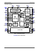
3 Oscillator
The Teridian 73S8010C device has an on-chip oscillator that can generate the smart card clock using an
external crystal, connected between the XTALIN and XTALOUT pins, to set the oscillator frequency.
When the card clock signal is available from another source, it can be connected to the pin XTALIN, and
the pin XTALOUT should be left unconnected.
4 DC-DC Converter – Card Power Supply
An internal DC-DC converter provides the card power supply. This converter is able to provide either a
3 V or 5 V card voltage from the power supply applied on the V
DD
pin. The digital ISO-7816-3 sequencer
controls the converter. Bit 2 of the Control register selects the card voltage.
The circuit is an inductive step-up converter/regulator. The external components required are 2 filter
capacitors on the power-supply input V
DD
(100 nF + 10 F, next to the LIN pin), an inductor, and an output
filter capacitor on the card power supply V
CC
. The circuit performs regulation by activating the step-up
operation when V
CC
is below a set point of 5.0 or 3.0 volts minus a comparator hysteresis voltage and the
input supply V
DD
is less than the set point for V
CC
. When V
DD
is greater than the set point for V
CC
(V
DD
=
3.6 V, V
CC
= 3 V) the circuit operates as a linear regulator. Depending on the inductor values, the voltage
converter can provide current on V
CC
as high as 100 mA.
The circuit provides over-current protection and limits I
CC
to 150 mA. When an over-current condition is
sensed, the circuit initiates a deactivation sequence from the control logic and reports back to the host
controller a fault on the interrupt output INT.
Choice of the Inductor
The nominal inductor value is 10 H, rated for 400 mA. The inductor is connected between pin LIN (pin 5
in the SO package, pin 2 in the QFN package) and the V
DD
voltage. The value of the inductor can be
optimized to meet a particular configuration (I
CC_MAX
). The inductor should be located on the PCB as
close as possible to the LIN pin of the IC.
Choice of the V
CC
Capacitor
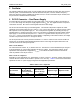
Depending on the applications, the requirements in terms of both V
CC
minimum voltage and transient
currents that the interface must be able to provide to the card vary. Table 4 shows the recommended
capacitors for each V
CC
power supply configuration and applicable specification.
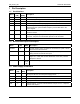
Table 4: Choice of Vcc Capacitor
Specification Requirement Application
Specification
Min V
CC
Voltage
Allowed During
Transient Current
Max Transient
Current Charge
Capacitor Type Capacitor Value
EMV 4.0 4.6V 30nA.s
X5R/X7R w/
ESR < 100 m
3.3 F
ISO-7816-3 4.5V 20nA.s
1 F