
Datasheet


DS_8010C_024 73S8010C Data Sheet
Rev. 1.5 7
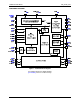
2 Host Interface (I
2
C Bus)
A fast-mode 400 kHz I
2
C bus slave interface is used for controlling the device and reading the status of
the device via the data pin SDA and clock pin SCL. The bus has 3 address select pins, SAD0, SAD1,
and SAD2. This allows up to 8 devices to be connected in parallel.
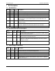
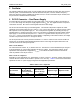
Table 1: Device Address Selections
SAD2 SAD1 SAD0 I
2
C Address (7 bits)
0 0 0 0x40
0 0 1 0x42
0 1 0 0x44
0 1 1 0x46
1 0 0 0x48
1 0 1 0x4A
1 1 0 0x4C
1 1 1 0x4E
Bit 0 of the I
2
C address is the R/W bit. Refer to Figure 2 and Figure 3 for usage.
2.1 Host Interface Control
Table 2 describes the Host Interface Control Register bits (power-on Reset = 0x00).
Table 2: Host Control Register
Name Bit Description
Start/Stop 0
When set, initiates an activation and a cold reset procedure; when reset, initiates
a deactivation sequence.
Warm reset 1
When set, initiates a warm reset procedure; automatically reset by hardware
when the card starts answering or when the card is declared mute.
5 V and 3 V 2 When set, V
CC
= 3 V; when reset, V
CC
= 5 V.
Clock Stop 3 When set, card clock is stopped. Bit 4 determines the card clock stop level.
Clock Stop
Level
4 When set, card clock stops high; when reset card clock stops low.
Clksel1 5
Bits 5 and 6 determine the clock rate to the card according to the following table.
CLKDIV1 CLKDIV2 Clock Rate
0 0 XTALIN/8
0 1 XTALIN/4
1 1 XTALIN/2
1 0 XTALIN
Clksel2 6
I/O enable 7
When set, data is transferred between I/O (AUX1, AUX2) and I/OUC (AUX1UC,
AUX2UC); when reset, I/O (AUX1, AUX2) and I/OUC (AUX1UC, AUX2UC) are
high impedance.
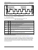
I
2
C-bus Write to the Control Register
The I
2
C-bus Write command to the control register follows the format shown in Figure 2.
After the START condition, the master sends a slave address. This address is seven bits long followed
by an eighth bit, which is an opcode bit (R/W) – a ‘zero’ indicates the master will write data to the control
register. After the R/W bit, the ’zero’ ACK bit is sent to the master by the device. The master now starts
sending the 8 bits of data to the control register during the DATA bits time. After the DATA bits, the ‘zero’