
Datasheet


73S8010R Data Sheet DS_8010R_022
6 Rev. 1.6
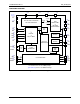
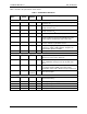
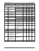
Table 1 describes the pin functions for the device.
Table 1: 73S8010R Pin Definitions
Pin
Name
Pin
(SO28)
Pin
(QFN32)
Type Description
Card Interface
I/O 11 8 IO Card I/O: Data signal to/from card. Includes a pull-up
resistor to V
CC.
AUX1 13 11 IO AUX1: Auxiliary data signal to/from card. Includes a
pull-up resistor to V
CC.
AUX2 12 10 IO AUX2: Auxiliary data signal to/from card. Includes a
pull-up resistor to V
CC.
RST 16 14 O Card reset: provides reset (RST) signal to card.
CLK 15 13 O Card clock: provides clock signal (CLK) to card. The
crystal oscillator frequency and CLKSEL bits in the
control register determine the rate of this clock.
PRES 10 7 I Card Presence switch: active high indicates card is
present. Includes a pull-down resistor.
VCC 17 15 PSO Card power supply – logically controlled by the
sequencer, output of LDO regulator. Requires an
external filter capacitor to GND.
GND 14 12 GND Card ground.
Miscellaneous Inputs and Outputs
XTALIN 24 23 I Crystal oscillator input: can be connected to crystal or
driven as a source for the card clock.
XTALOUT 25 24 O Crystal oscillator output: connected to crystal. Left
open if XTALIN is being used as an external clock
input.
VDDF_ADJ 18 17 I V
DD
threshold adjustment input: this pin can be used
to overwrite a higher VDDF value (that controls
deactivation of the card). Must be left open if unused.
NC 7, 8, 9 4,5,6,9,
16,25,32
–
Non-connected pin.
Power Supply and Ground
VDD 21 20 System interface supply voltage and supply voltage
for internal circuitry.
VPC 6 3 LDO regulator power supply source.
GND 4 1 GND LDO regulator ground.
GND 14 12 GND Smart card I/O ground.
GND 5, 22 2,21 GND Digital ground.