
Datasheet


DS_8010R_022 73S8010R Data Sheet
Rev. 1.6 7
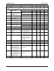
Pin
Name
Pin
(SO28)
Pin
(QFN32)
Type Description
Microcontroller Interface
INT 23 22 O Interrupt output signal (negative assertion) to the
processor. A 20 kΩ pull up to V
DD
is provided
internally.
SAD0
SAD1
SAD2
1
2
3
29
30
31
I
I
I
Serial device address bits. Digital inputs for address
selection that allows for the connection of up to 8
devices in parallel. Address selections is as follows:
SAD2 SAD1 SAD0
(7 bit) I
2
C
Address
0
0
0
0x40
0
0
1
0x42
0 1 0 0x44
0 1 1 0x46
1 0 0 0x48
1 0 1 0x4A
1 1 0 0x4C
1 1 1 0x4E
Pins SAD0 and SAD1 are internally pulled down and
SAD2 is internally pulled up. The default address
when unconnected is 0x48.
SCL 19 18 I I
2
C clock signal input.
SDA 20 19 I/O I
2
C bi-directional serial data signal.
I/OUC 26 26 IO System controller data I/O to/from the card. Includes
an internal pull-up resistor to V
DD.
AUX1UC 27 27 IO System controller auxiliary data I/O to/from the card.
Includes an internal pull-up resistor to V
DD.
AUX2UC 28 28 IO System controller auxiliary data I/O to/from the card.
Includes an internal pull-up resistor to V
DD.