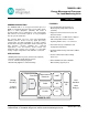
78M6610+LMU Energy Measurement Processor for Load Monitoring Units DATA SHEET GENERAL DESCRIPTION FEATURES The 78M6610+LMU is an energy measurement processor (EMP) for load monitoring and control of any 2-wire singlephase or 3-wire split-phase (120/180°) AC circuit. It provides flexible sensor configuration of four analog inputs and numerous host interface options for easy integration into any system architecture.
78M6610+LMU Data Sheet Table of Contents Electrical Specifications ............................................................................................................................. 5 ABSOLUTE MAXIMUM RATINGS ....................................................................................................... 5 Recommended External Components .................................................................................................. 5 Recommended Operating Conditions ...................
78M6610+LMU Data Sheet Active Power (P) ....................................................................................................................... 31 Reactive Power (Q) ................................................................................................................... 32 Apparent Power (S) ................................................................................................................... 32 Power Factor (PF) .......................................................
78M6610+LMU Data Sheet Table of Figures Figure 1. SPI Timing ........................................................................................................................ 8 2 Figure 2. I C Timing ......................................................................................................................... 9 Figure 3. QFN Package Pinout ...................................................................................................... 10 Figure 4. Package Outline ...................
78M6610+LMU Data Sheet Electrical Specifications ABSOLUTE MAXIMUM RATINGS (All voltages with respect to ground.) Supplies and Ground Pins: V3P3D, V3P3A -0.5V to +4.6V GNDD, GNDA -0.5V to +0.5V Analog Input Pins: -10mA to +10mA -0.5V to (V3P3 + 0.5V) A0, A1, A2, A3, A4, A5 Oscillator Pins: -10mA to +10mA -0.5V to +3.0V XIN, XOUT Digital Pins: IFC0, IFC1, SSB/DIR/SCL, SDO/TX/SDAO, SDI/RX/SDAI, RESET, SCK/ADDR0, MP10, MP0, MP4, MP6/ADDR1, MP7 -30mA to +30mA, -0.5V to (V3P3D + 0.
78M6610+LMU Data Sheet Performance Specifications Note that production tests are performed at room temperature. Input Logic Levels PARAMETER CONDITIONS Digital High-Level Input Voltage (VIH) MIN TYP MAX 2 UNITS V Digital Low-Level Input Voltage (VIL) 0.8 V MAX UNITS Output Logic Levels PARAMETER Digital High-Level Output Voltage (VOH) Digital Low-Level Output Voltage (VOL) CONDITIONS MIN TYP ILOAD = 1mA V3P3 0.4 V ILOAD = 10mA V3P3 0.6 V ILOAD = 1mA 0 0.4 V 0.
8M6610+LMU Data Sheet ADC Converter, V3P3 Referenced LSB values do not include the 9-bit left shift at EMP input. CONDITIONS PARAMETER Usable Input Range (VIN - V3P3) THD (First 10 Harmonics) Input Impedance Temperature Coefficient of Input Impedance ADC Gain Error vs. %Power Supply Variation 106 ∆Nout PK 357nV / VIN 100 ∆V 3P3 A / 3.3 7 TYP -250 VIN = 65Hz, 64kpts FFT, Blackman-Harris window VIN = 65Hz MAX UNITS +250 mV peak dB -85 30 VIN = 65Hz (Note 1) 90 -10 kΩ Ω/°C 1.
78M6610+LMU Data Sheet Timing Specifications Reset PARAMETER CONDITIONS MIN TYP MAX UNITS Reset Pulse Fall Time (Note 1) 1 µs Reset Pulse Width (Note 1) 5 µs SPI Slave Port PARAMETER CONDITIONS MIN TYP MAX UNITS SCK Cycle Time (tSPIcyc) 1 µs Enable Lead Time (tSPILead) 15 ns Enable Lag Time (tSPILag) 0 ns SCK Pulse Width (tSPIW) High 250 Low 250 ns SSB to First SCK Fall (tSPISCK) Ignore if SCK is low when SSB falls (Note 1) 2 ns Disable Time (tSPIDIS) (Note 1) 0 ns
78M6610+LMU Data Sheet 2 I C Slave Port (Note 1) PARAMETER CONDITIONS MIN Bus Idle (Free) Time Between Transmissions (STOP/START) (tBUF) TYP MAX 1500 UNITS ns 2 (Note 2) 20 300 ns 2 (Note 2) 20 300 ns I C Input Fall Time (tICF) I C Input Rise Time (tICR) 2 I C START or Repeated START Condition Hold Time (tSTH) 500 ns 600 ns 2 600 ns 2 1300 ns 2 100 ns 2 10 ns 2 I C START or Repeated START Condition Setup Time (tSTS) I C Clock High Time (tSCH) I C Clock Low Time (tSCL) I
78M6610+LMU Data Sheet 21 A0 22 A1 23 V3 P 3 A A3 24 A2 A4 Pin Configuration 20 19 A5 1 18 RESET GNDA 2 17 IFC1 IFC0 3 16 MP10 MP7 4 15 MP0 MP6/ADDR1 5 14 SCK/ADDR0 SSB/DIR/SCL 6 78 M 6610 + LMU ( Top ) 10 11 12 XOUT GNDD SDO/TX/SDAO V3 P 3 D MP4 9 XIN 8 7 13 SDI/RX/SDAI Figure 3.
78M6610+LMU Data Sheet Package Information For the latest package outline information and land patterns (footprints), go to www.maximintegrated.com/packages. Note that a “+”, “#”, or “-” in the package code indicates RoHS status only. Package drawings may show a different suffix character, but the drawing pertains to the package regardless of RoHS status. PACKAGE TYPE 24 TQFN PACKAGE CODE OUTLINE NO. LAND PATTERN NO. T2444+4 21-0139 90-0022 Figure 4.
78M6610+LMU Data Sheet On-Chip Resources Overview The 78M6610+LMU device integrates all the hardware blocks required for accurate AC power and energy measurement.
78M6610+LMU Data Sheet Clock Management The device can be clocked by either a trimmed internal RC oscillator or by oscillator circuitry that relies on an external crystal. The internal RC oscillator provides an accurate clock source for UART baud rate generation. Only time based calculations such as line frequency and watt-hour (energy) are affected by clock accuracy. The chip hardware automatically handles the clock sources logic and distributes the clock to the rest of the device.
78M6610+LMU Data Sheet Power-On and Reset Circuitry An on-chip power-on reset (POR) block monitors the supply voltage (V3P3D) and initializes the internal digital circuitry at power-on. Once V3P3D is above the minimum operating threshold, the POR circuit triggers and initiates a reset sequence. It will also issue a reset to the digital circuitry if the supply voltage falls below the minimum operating level. In addition to the internal sources, a reset can be forced by applying a low level to the RESET pin.
78M6610+LMU Data Sheet Analog Front-End and Conversion The Analog Front-End (AFE) includes an input multiplexer, optional pre-amplifier gain stage, Delta-Sigma A/D Converter, bias current references, voltage references, temperature sensor, and several voltage fault comparators. Analog Inputs Up to four external sensors can be connected to the 78M6610+LMU. Two single-ended inputs are available for voltage sensors and two differential pairs are available for connecting current sensors.
78M6610+LMU Data Sheet Functional Description and Operation This section describes the operation and configuration of the 78M6610+LMU. It includes the flow of measurement data, relevant calculations, alarm monitoring, I/O control, and user configurations. Measurement Interface The 78M6610+LMU incorporates a flexible measurement interface for simplified integration into any single-phase system. This section describes the configuration and signal conditioning of the analog inputs.
78M6610+LMU Data Sheet High Pass Filters and Offset Removal Offset registers for each analog input contain values to be subtracted from the raw ADC outputs for the purpose of removing inherent system DC offsets from any calculated power and RMS values. These registers are signed fixed point numbers with a possible range of -1.0 to 1 - LSB. They default to 0 and can be manually changed by the user or integrated offset calibration routines.
78M6610+LMU Data Sheet Gain Correction The system (sensors) and the 78M6610+LMU device inherently have gain errors that can be corrected by using the gain registers. These registers can be directly accessed and modified by an external processor or automatically updated by an integrated self calibration routine. Input gain registers are signed fixed point numbers with the binary point to the left of bit 21. They are set to 1.
78M6610+LMU Data Sheet Phase Compensation Phase compensation registers are used to compensate for phase errors or time delays between the voltage input source and respective current source that are introduced by the off-chip sensor circuit. The user configurable registers are signed fixed point numbers with the binary point to the left of bit 21. Values are in units of high rate (4kHz) sample delays so each integer unit of delay is 250µs with a total possible delay of ±4 samples (roughly ±20° at 60Hz).
78M6610+LMU Data Sheet Voltage Input Configuration The 78M6610+LMU supports multiple analog input configurations for determining the three potential voltage sources in a split-phase circuit. The device measures the voltage difference between any two references and uses this information to derive the voltages VA, VB, and VC as shown below. Conductor A + + VA - Conductor N VC VB + Conductor B - Figure 9.
78M6610+LMU Data Sheet Two example configurations are shown below. For determining the sign of S0 or S2 measurements, one should note that results for single ended inputs are referenced to V3P3. Conductor A 78M6610+LMU S0 V3P3 A0 Conductor N S2 A1 VA = +1*S0 +0*S2 VB = +0*S0 +1*S2 VC = +1*S0 -1*S2 Conductor B V3P3 Conductor A 78M6610+LMU S0 A0 VA = -1*S0 +0*S2 VB = +1*S0 -1*S2 VC = +0*S0 -1*S2 Conductor N S2 A1 Conductor B Figure 11.
78M6610+LMU Data Sheet Voltage Input Flowchart The figure below illustrates the computational flowchart for VA, VB, and VC. The values for voltage input configuration register can be saved in flash memory and automatically restored at power-on or reset.
78M6610+LMU Data Sheet Current Input Configuration The 78M6610+LMU supports multiple analog input configurations for determining the two load currents in a split-phase AC circuit. The device measures the current of any two conductors and uses this information to derive the load currents shown below. IA Conductor A IA= - IB - IN IB= - IA - IN IN Conductor N IB Conductor B Figure 13.
78M6610+LMU Data Sheet Current Configuration Examples IA Conductor A 78M6610+LMU S1 A3 IN A2 Conductor N A4 A5 S3 Conductor B IA = +1*S1 +0*S3 IB = +0*S1 +1*S3 IB IA Conductor A IN 78M6610+LMU A3 S1 A2 IA = +1*S1 +0*S3 IB = -1*S1 -1*S3 Conductor N S3 A5 A4 Conductor B IB Figure 15. Current Configuration Examples Pre-Amp By default, the full-scale signal that can be applied to the current inputs is V3P3A ±250mVpk (176.78mVRMS).
78M6610+LMU Data Sheet Current Input Flowchart The figure below illustrates the computational flowchart for IA and IB. The values for current input configuration register can be saved in flash memory and automatically restored at power-on or reset. gain_adj HPF_COEF_I CONFIG S1_OFF S1_GAIN 2, 1, -1, 0 CONFIG S1 X HPF X8 X Delay Compensation X S3_OFF S3_GAIN 2, 1, -1, 0 CONFIG S3 X8 HPF X X Delay Compensation X + IA + IB CONFIG 2, 1, -1, 0 X 2, 1, -1, 0 X Figure 16.
78M6610+LMU Data Sheet Data Refresh Rates Instantaneous Voltage, Current, Power, and Quadrature measurement results are updated at the sample rate of 4kS/s and are generally not useful unless accessed with a high speed interface such as SPI. The CYCLE register is a 24-bit counter that increments every high-rate sample update and resets when low-rate results are updated. Low-rate results, updated at a user configurable rate, are typically used and more suitable for most applications.
78M6610+LMU Data Sheet Calibration The 78M6610+LMU provides integrated calibration routines to modify gain and offset coefficients. The user can set up and initiate a calibration routine through the Command Register. When in calibration mode, the line-lock bit should be set for best results. The calibration routines will write the new coefficients to the relevant registers. The user can then save the new coefficients into flash memory as defaults using the flash access command in the Command Register.
78M6610+LMU Data Sheet Voltage Channel Measurements Instantaneous and quadrature voltage measurements are updated every sample while RMS Voltage and Peak Voltage are updated every accumulation interval (n samples). An AC voltage frequency measurement is also updated every low-rate interval.
78M6610+LMU Data Sheet Current Channel Measurements In addition to instantaneous current measurements updated every sample, Peak Current, RMS Current, and Crest Factor are updated every accumulation interval (n samples). Register Description Time Scale IA IB Instantaneous Current 1 sample IA_PEAK IB_PEAK Peak Current IA_RMS IB_RMS RMS Current IA_CREST IB_CREST Current Crest Factor 1 interval Peak Current This output is a capture of the largest magnitude instantaneous current load sample.
78M6610+LMU Data Sheet RMS Current The 78M6610+LMU reports true RMS measurements for current inputs. The RMS current is obtained by performing the sum of the squares of the instantaneous current samples over the accumulation interval and then performing a square root of the result after dividing by the number of samples in the interval. An optional “RMS offset” for the current channels can be adjusted to reduce errors due to noise or system offsets (crosstalk) exhibited at low input amplitudes.
78M6610+LMU Data Sheet Power Calculations This section describes the detailed flow of power calculations in the 78M6610+LMU. Generic equations for AC power measurement are listed in the table below.
78M6610+LMU Data Sheet Reactive Power (Q) Instantaneous reactive power results (PQA, PQB) are calculated by multiplying the instantaneous samples of current and the instantaneous quadrature voltage. The sum of these results are then averaged over N samples (accumulation time) to compute the average reactive power (VAR_A, VAR_B), and the aggregate average reactive power (VAR_C). A reactive power offset (Qx_OFFS) is also provided for each channel.
78M6610+LMU Data Sheet Fundamental and Harmonic Calculations The 78M6610+LMU includes the ability to separate low-rate voltage, current, active power, and reactive power measurement results into fundamental and total harmonic components. These outputs can also be used to track individual harmonics as well as the total value excluding the selected harmonic.
78M6610+LMU Data Sheet Energy Calculations Energy calculations are included in the 78M6610+LMU to minimize the traffic on the host interface and simplify system design. Low-rate power measurement results are multiplied by the number of samples (DIVISOR) to calculate the energy in the last accumulation interval. Energy results are summed together until a user defined “bucket size” is reached. When every bucket of energy is reached, the value in the energy counter register is incremented by one.
78M6610+LMU Data Sheet Example In this example the scaling registers are set as follows: VFSCALE = 667 (667V); IFSCALE = 50 (50A) In order to set the energy bucket to one Wh: 𝐵𝑢𝑐𝑘𝑒𝑡 = 3600 ∗ 4000 = 431.784 667 ∗ 50 The value to enter in the bucket register should be set as: 𝐵𝑢𝑐𝑘𝑒𝑡 𝑅𝑒𝑔𝑖𝑠𝑡𝑒𝑟 = 431.
78M6610+LMU Data Sheet Min/Max Tracking The 78M6610+LMU provides a set of output registers for tracking the minimum and/or maximum values of up to six (6) different low-rate measurement results over multiple accumulation intervals. The user can select which measurements to track through an address table. MM_ADDR# uses word addressing for all host interfaces. Register Description Time Scale Word addresses to track minimum and maximum values. A value of zero will disable tracking for that address slot.
78M6610+LMU Data Sheet Alarm Monitoring Low-rate alarm conditions are determined every accumulation interval. If results for Die Temperature, AC Frequency, or RMS Voltage exceeds or drops below user configurable thresholds, then a respective alarm bit in the STATUS register is set. For RMS Current and Watts results, maximum thresholds are provided for detecting over current or over power conditions with the load. Register Description T_MAX Threshold value which Temperature must exceed to trigger alarm.
78M6610+LMU Data Sheet SAG_THRESHOLD Figure 25. Voltage Sag Register Description VSAG_VAL Threshold value (in RMS) which voltage must go below to trigger a Sag alarm. VSURG_VAL Threshold value which voltage must go above to trigger alarm.
78M6610+LMU Data Sheet Status Registers The STATUS register is used to monitor the status of the device and user configurable alarms. All other registers mentioned in this section share the same bit descriptions. The STICKY register determines which alarm/status bits are sticky and which track the current status of the condition. Each alarm bit defined as sticky will (once triggered) hold its alarm status until the user clears it using the STATUS_RESET register.
78M6610+LMU Data Sheet Digital IO Functionality The DIO_STATE register contains the current status of the DIOs. The user can use this register to read the state of a DIO (if configured as an input) or control the state of the DIO (if configured as an output). The DIO_DIR register sets the direction of the pins, where “1” is input and “0” is output. If a DIO defined as an input is unconnected, internal pullups will assert the respective DIO bit in the DIO_STATE register.
78M6610+LMU Data Sheet Multipurpose (MP) Pins The 78M6610+LMU provides five MASK registers for signaling the status of any STATUS bit to one of five multipurpose (MP) DIO pins. These MASK registers have the same bit mapping as the STATUS register. The user must first enable the respective MP pin as an output before the DIO can be driven to its active state.
78M6610+LMU Data Sheet Command Register This register is used to issue commands to perform specific tasks to the device. Use of any command not listed in this document can cause unpredictable and possibly dangerous behavior. General Settings The general settings allows the user to enable functions such as UART auto reporting, relay operations, and Line Lock mode, etc. These settings are used with all other commands and are stored as non-volatile settings upon use of the Save to Flash Command (0xACC2xx).
78M6610+LMU Data Sheet Save to Flash Command (0xACC2xx) Use this command to save to flash the calibration coefficients and system defaults contained in the some of the input registers. Upon reset or power-on, the values stored in flash becomes new system defaults. The General Settings bits ([7:0] are stored in nonvolatile storage while the upper 16 bits (23:16]) are stored as 0x0000 (No Action Command). When the process completes, bits [23:8] are cleared.
78M6610+LMU Data Sheet Calibration Command (0xCAxxxx) Use this command to start the calibration process for the selected inputs. It is assumed that appropriate input signals are applied before starting calibration. When the calibration process completes, bits [23:16] are cleared along with bits associated with channels that calibrated successfully. Any channels that failed will have their corresponding bit left set.
78M6610+LMU Data Sheet The remaining bits configure which the sensor inputs are used to derive line voltages and load currents. CONFIG Bits 19:18 17:16 15:14 13:12 11:10 9:8 7:6 5:4 3:2 1:0 Multiplier M2 M0 M2 M0 M2 M0 M3 M1 M3 M1 Source VC VB VA IB IA There are four choices for every M value as shown below. See Section 2.1 for more information.
78M6610+LMU Data Sheet Register Access All user registers are contained in a 256-word (24-bits each) area of the on-chip RAM and can be accessed 2 through the UART, SPI, or I C interfaces. These registers are byte-addressable via the UART interface and word2 addressable via the SPI, and I C interfaces. These registers consist of read (output), write (input), and read/write in the case of the Command Register.
78M6610+LMU Data Sheet Register Locations 2 Use Word addresses for I C and SPI interfaces and Byte addresses for the SSI (UART) protocol. Nonvolatile (NV) register defaults are indicated with a ‘Y’. All other registers are initialized as described in the Functional Description.
78M6610+LMU Data Sheet Word Byte Addr Addr 29 7B 2A 7E 2B 81 2C 84 2D 87 2E 8A 2F 8D 30 90 31 93 32 96 33 99 34 9C 35 9F 36 A2 37 A5 38 A8 39 AB 3A AE 3B B1 3C B4 3D B7 3E BA 3F BD 40 C0 41 C3 42 C6 43 C9 44 CC 45 CF 46 D2 47 D5 48 D8 49 DB 4A DE 4B E1 4C E4 4D E7 4E EA 4F ED 50 F0 51 F3 52 F6 53 F9 54 FC 55 FF 56 102 57 105 58 108 Register Type NV VRMS_MIN VRMS_MAX VA_RMS VB_RMS VA_FUND VB_FUND VA_HARM VB_HARM VC_RMS – VA VB VQA VQB VC SINE COSINE VA_PEAK VB_PEAK ITARGET IRMS_MIN IA_RMS IB_RMS IA_FUND
78M6610+LMU Data Sheet Word Byte Addr Addr 59 10B 5A 10E 5B 111 5C 114 5D 117 5E 11A 5F 11D 60 120 61 123 62 126 63 129 64 12C 65 12F 66 132 67 135 68 138 69 13B 6A 13E 6B 141 6C 144 6D 147 6E 14A 6F 14D 70 150 71 153 72 156 73 159 74 15C 75 15F 76 162 77 165 78 168 79 16B 7A 16E 7B 171 7C 174 7D 177 7E 17A 7F 17D 80 180 81 183 82 186 83 189 84 18C 85 18F 86 192 87 195 49 Register Type QFUND_B QHARM_A QHARM_B PA PB PQA PQB WATT_MAX PA_OFFS QA_OFFS PB_OFFS QB_OFFS PFA PFB PFC – TEMPC T_TARGET T_MIN T_MAX
78M6610+LMU Data Sheet Word Byte Addr Addr 88 198 89 19B 8A 19E 8B 1A1 8C 1A4 8D 1A7 8E 1AA 8F 1AD 90 1B0 91 1B3 92 1B6 93 1B9 94 1BC 95 1BF 96 1C2 97 1C5 98 1C8 99 1CB 9A 1CE 9B 1D1 9C 1D4 9D 1D7 9E 1DA 9F 1DD A0 1E0 A1 1E3 A2 1E6 A3 1E9 A4 1EC A5 1EF A6 1F2 A7 1F5 A8 1F8 A9 1FB AA 1FE AB 201 AC 204 AD 207 AE 20A AF 20D B0 210 B1 213 B2 216 B3 219 Register Type NV Description SCRATCH4 BUCKET BUCKET IA_CREST IB_CREST – – PA_POS_CNT – – PA_NEG_CNT – – PB_POS_CNT – – PB_NEG_CNT – – PQA_POS_CNT – – PQA_NE
78M6610+LMU Data Sheet Serial Interfaces All user registers are contained in a 256-word (24-bits each) area of the on-chip RAM and can be accessed 2 through the UART, SPI, or I C interfaces. While access to a single byte is possible with some interfaces, it is highly recommended that the user access words (or multiple words) of data with each transaction. Only one interface can be active at a time. The interface selection pins are sampled at the end of a reset sequence to determine the operating mode.
78M6610+LMU Data Sheet Device Address Configuration The SSI protocol utilizes 8-bit addressing for multipoint communications. The usable SSI ID range is 1 to 255. In multipoint systems with more than 4 targets, the user must configure device address bits in the DEVADDR according to the formula SSI ID = Device Address +1. A device address of 'FF' is not supported. DEVADDR [23:6] bits are not used and must be set to 1.
78M6610+LMU Data Sheet SSI Protocol Description The SSI protocol is command response system supporting a single master and one or more targets. The host (master) sends commands to a selected target that first verifies the integrity of the packet before sending a reply or executing a command. Failure to decode a host packet will cause the selected target to send a fail code. If the condition of a received packet is uncertain, no reply is sent. Each target must have a unique SSI ID.
78M6610+LMU Data Sheet Master Packets Master packets always start with the 1-byte header (0xAA) for synchronization purposes. The master then sends the byte count of the entire packet (up to 255 byte packets) followed by the payload (up to 253 bytes) and a 1byte modulo-256 checksum of all packet bytes for data integrity checking. Figure 30. Master Packet Structure The payload can contain either a single command or multiple commands if the target is already selected.
78M6610+LMU Data Sheet Command Payload Examples Device Selection PAYLOAD SSI ID 0xCF Command Register Address Pointer Selection PAYLOAD 0xA3 Command Register Address (2 Bytes) Small Read Command (3 bytes) PAYLOAD 0xE3 Command Large Read Command (30 bytes) PAYLOAD 0xE0 Command 0x1E (30 bytes) Small Write Command (3 bytes) PAYLOAD 0xD3 Command 3 Bytes of Data Large Write Command (30 bytes) Byte Count 0x21 (34 bytes) PAYLOAD 0xD0 Command 30 Bytes of Data After each read or write operation, the inter
78M6610+LMU Data Sheet Slave Packets The type of slave packet depends upon the type of command from the master device and the successful execution by the slave device. Standard replies include “Acknowledge” and “Acknowledge with Data”. ACKNOWLEDGE without data ACKNOWLEDGE with data BYTE COUNT READ DATA CHECK SUM If no data is expected from the slave or there is a fail code, a single byte reply is sent.
78M6610+LMU Data Sheet SPI Interface The Maxim device operates as a SPI slave. The host is expected to instigate and control all transactions.
78M6610+LMU Data Sheet Single Word SPI Reads The device supplies direct read access to the device RAM memory. To read the RAM the master device must send a read command to the slave device and then clock out the resulting read data. SSB must be kept active low for the entire read transaction (command and response). SCK may be interrupted as long as SSB remains low. ADDR[5:0] is filled with the word address of the read transaction. RAM data contents are transmitted most significant byte first.
78M6610+LMU Data Sheet Single Word SPI Writes The device supplies direct write access to the device RAM memory. To write the RAM the master device must send a write command to the slave device and then clock out the write data. SSB must be kept active low for the entire write transaction (command and data). SCK may be interrupted as long as SSB remains low. ADDR[5:0] is filled with the word address of the write transaction. RAM data contents are transmitted most significant byte first.
78M6610+LMU Data Sheet I2C Interface 2 The 78M6610+LMU has an I C interface available at the SDAI, SDAO, and SCL pins. The interface 2 supports I C slave mode with a 7-bit address and operates at a data rate up to 400kHz. The figure below shows two possible configurations. Configuration A is the standard configuration. The double pin for SDA also allows for isolated configuration B.
78M6610+LMU Data Sheet Bus Characteristics • A data transfer may be initiated only when the bus is not busy. • During data transfer, the data line must remain stable whenever the clock line is HIGH. Changes in the data line while the clock line is HIGH will be interpreted as a START or STOP condition. Bus Conditions: • Bus Not Busy (I): Both data and clock lines are HIGH indicating an Idle Condition.
78M6610+LMU Data Sheet Write Operations Following the START (S) condition from the master, the device address (7-bits) and the R/W bit (logic low for write) are clocked onto the bus by the master. This indicates to the addressed slave receiver that the register address will follow after it has generated an acknowledge bit (A) during the ninth clock cycle. Therefore, the next byte transmitted by the master is the register address and will be written into the address pointer of the 78M6610+LMU.
78M6610+LMU Data Sheet Read Operations Read operations are initiated in the same way as write operations with the exception that the R/W bit of the control byte is set to one. There are two basic types of read operations: current address read and random read. Current Address Read: the 78M6610+LMU contains an address counter that maintains the address of the last register accessed, internally incremented by one when the stop bit is received.
78M6610+LMU Data Sheet Ordering Information PART 78M6610+LMU/B01 78M6610+LMU/B01T TEMP RANGE -40°C to +85°C -40°C to +85°C PIN-PACKAGE 24-QFN 24-QFN TOP MARK EMP EMP +Denotes a lead(Pb)-free/RoHS-compliant package. T = Tape and reel. Contact Information For more information about the 78M6610+LMU or other Maxim Integrated products, go to: www.maximintegrated.com/support.
78M6610+LMU Data Sheet Revision History REVISION NUMBER REVISION DATE 0 1/13 Initial release 1 4/14 Updated Command Register and SPI Interface sections 2 8/14 Updated Storage Temperature parameter on the Electrical Characteristics table and SPI Interface section DESCRIPTION PAGES CHANGED — 42–45, 57–59 5, 57–59 Maxim Integrated cannot assume responsibility for use of any circuitry other than circuitry entirely embodied in a Maxim Integrated product. No circuit patent licenses are implied.
Rev.