
Datasheet
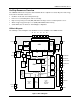
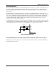
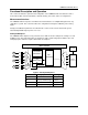
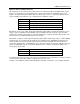
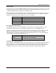

Table Of Contents
- Electrical Specifications
- Pin Configuration
- On-Chip Resources Overview
- Functional Description and Operation
- Measurement Interface
- Data Refresh Rates
- Scaling Registers
- Calibration
- Voltage Channel Measurements
- Current Channel Measurements
- Power Calculations
- Fundamental and Harmonic Calculations
- Energy Calculations
- Min/Max Tracking
- Alarm Monitoring
- Status Registers
- Digital IO Functionality
- Command Register
- Control Register
- Configuration Register
- Register Access
- Serial Interfaces
- Ordering Information
- Contact Information
- Revision History
78M6610+LMU Data Sheet
Voltage Input Configuration
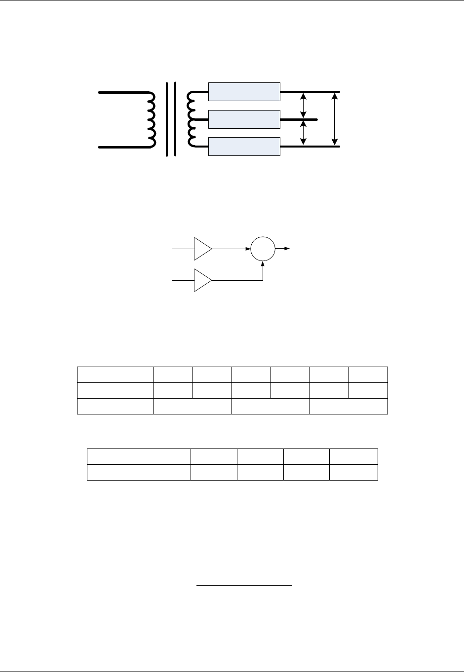
The 78M6610+LMU supports multiple analog input configurations for determining the three potential
voltage sources in a split-phase circuit. The device measures the voltage difference between any two
references and uses this information to derive the voltages VA, VB, and VC as shown below.
Conductor A
Conductor N
Conductor B
VA
VB
VC
+
+
+
-
-
-
Figure 9. Voltage Input Configuration
Each calculated voltage source (VA, VB, and VC) is derived from the following user configurable function
of the voltage input multiplexer slots (S0, S2) and three pairs of multiplier values (M0, M2). This function
derives source voltages VA, VB, and VC by summing S0 x M0 and S2 x M2.
M0
+
M2
VxS0
S2
Figure 10. Voltage Computation
The user sets the multiplier values M0 and M2 for each voltage source in the CONFIG register using the
model where a one (1) value adds the input, a two (2) value adds two of the input, a minus one (-1) value
subtract the input, a zero (0) value does not include the input.
CONFIG Bits 19:18 17:16 15:14 13:12 11:10 9:8
Multiplier M2 M0 M2 M0 M2 M0
Source VC VB VA
There are four choices for every M value as shown below.
Multiplier Bits 00 01 10 11
M (multiplier) Value -1 0 1 2
The output registers VA, VB, and VC are automatically scaled by a factor of 0.5 if M0 and M2 are both
nonzero.
For example, by setting the multiplier bits as follows:
= +1 0 1 2
The effective content of the Vc register would result in:
=
(
+1 0
)
+ (1 2)
2
This scaling is done to prevent the output register from overflowing.
20 Rev 2