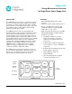
78M6610+PSU Energy Measurement Processor for Single-Phase Power-Supply Units DATA SHEET FEATURES DESCRIPTION The 78M6610+PSU is a single-core energy measurement processor for single-phase power supplies. It is designed specifically for real-time monitoring at the input of AC/DC power converters used in data centers and IT server rooms. It is available in either a 24-pin QFN or 16-pin TSSOP package for optimal space savings.
78M6610+PSU Data Sheet Table of Contents 1 On-Chip Resources Overview ........................................................................................................... 5 1.1 Clock Management ...................................................................................................................... 6 1.2 Power-On Reset, WD Timer, and Reset Circuitry ....................................................................... 7 1.3 Analog Front-End and Conversion ............................
78M6610+PSU Data Sheet 3.8 3.7.7 Alarm Counter Registers ............................................................................................... 37 Command Register .................................................................................................................... 38 3.8.1 General Settings ............................................................................................................ 38 3.8.2 No Action (0x00xxxx) .......................................................
78M6610+PSU Data Sheet Figure 4-2: Signal Timing on the SPI Bus ...................................................................................... 48 Figure 4-3: Single Word Read Access Timing ............................................................................... 49 Figure 4-4: Single Word Write Access Timing ............................................................................... 50 2 Figure 4-5: I C Bus Connection in Standard (A) and Isolated (B) Configuration .........................
78M6610+PSU Data Sheet 1 On-Chip Resources Overview The 78M6610+PSU integrates all the functional hardware blocks required to embed solid-state AC power and energy measurement.
78M6610+PSU Data Sheet 1.1 Clock Management The 78M6610+PSU can be clocked by either the trimmed internal RC oscillator or by oscillator circuitry that relies on an external crystal. The 78M6610+PSU hardware automatically handles the clock sources logic and distributes the clock to the rest of the device.
8M6610+PSU Data Sheet 1.2 Power-On Reset, WD Timer, and Reset Circuitry Power-On Reset (POR) An on-chip Power-On Reset (POR) block monitors the supply voltage (V3P3D) and initializes the internal digital circuitry at power-on. Once V3P3D is above the minimum operating threshold, the POR circuit triggers and initiates a reset sequence. It will also issue a reset to the digital circuitry if the supply voltage falls below the minimum operating level.
78M6610+PSU Data Sheet 1.3 Analog Front-End and Conversion The Analog Front-End (AFE) of the 78M6610+PSU includes an input multiplexer, delta-sigma A/D converter, bias current references, voltage references, temperature sensor, and several voltage fault comparators. Delta-Sigma A/D Converter A second-order delta-sigma converter digitizes the analog inputs. The converted data is then processed through an FIR filter.
78M6610+PSU Data Sheet 1.7 Multi-Purpose Digital I/O Pins The MP0 and MP1 input/output pins are not currently used. The pins have an internal pull-up and can be left floating. 1.8 Alarm Pins (ACFAULT, ACCRIT) Alarm pins are available to signal an alarm condition has been reached. Table 1-1 shows the available alarm pins and the intended usage. The alarm thresholds and conditions are programmable through dedicated registers. The status of each individual alarm is accessible through a status register.
78M6610+PSU Data Sheet 2 Functional Description and Operation This section describes the 78M6610+PSU functionality. It includes measurements and relevant calculations, alarms, auxiliary functions such as calibrations, zero-crossing, relay control, etc. A set of input (write), output (read) and read/write registers are provided to allow access to calculated data and alarms and to configure the device. The input (write) registers values can be saved into flash memory through a specific command.
78M6610+PSU Data Sheet 2.2 Current and Voltage RMS Calculations The 78M6610+PSU provides true RMS measurements for both current and voltage inputs. The RMS is obtained by performing the square sum of the instantaneous samples of voltage and current over a time interval (commonly referred as accumulation time) and then performing a square root of the result after dividing by the number of samples in the time interval.
78M6610+PSU Data Sheet 2.3 Power Calculations and Power Factor The 78M6610+PSU computes the active, reactive, and apparent power. In addition, the 78M6610+PSU computes the fundamental power, determined only by the fundamental components of the voltage and current and the harmonic power, determined by the harmonic components of the voltage and current. 2.3.1 Active Power Calculation Active power is calculated as the product of the voltage and current waveforms.
78M6610+PSU Data Sheet 2.4 Fundamental and Harmonics Calculations Fundamental and Harmonics The 78M6610+PSU provides measurements on fundamental and total harmonic of voltage, current, and power (active, reactive, and apparent).
78M6610+PSU Data Sheet It is also possible to set the accumulation interval based on a number of AC Voltage line cycles. If the Line Lock (LL) Command register bit is set and AccumCyc register is non-zero then the device will calculate, on every frequency update, a new Accum value based upon the line frequency.
78M6610+PSU Data Sheet 2.8 Voltage and Current Min/Max and Peak Tracking 2.8.1 Voltage and Current Min/Max Tracking The 78M6610+PSU allows recording the lowest and highest voltage and current rms values. These values are stored in the registers Vhi, Vlo, Ihi, and Ilo. To reset these values it is necessary to write to these registers. For example, a value of 0x000000 should be written in the Vhi or Ihi register in order to reset them.
78M6610+PSU Data Sheet 2.9.2 I/R Voltage Drop Compensation The PCB traces have a certain resistance that at high loads causes a voltage drop from the inlet to the measurement point. The voltage drop causes an error in the voltage and power measurements. The correction is proportional to the current measured. A coefficient proportional to the input stage resistance is available and tunable by the user. Usually this coefficient is set by the user for a specific hardware and does not require calibration. 2.
78M6610+PSU Data Sheet 2.11 Voltage Sag and Surge Detection The 78M6610+PSU implements a voltage sag detection function, which can generate an alarm when the line voltage drops below a programmable threshold. The firmware calculates on a sample-by-sample basis the trailing mean square of the input voltage: 𝑉𝑀𝑆 𝑓𝑙𝑖𝑛𝑒 = 2 × 𝑓𝑠𝑎𝑚𝑝𝑙𝑒 × 0 � 𝑛= −𝑖𝑛𝑡( 𝑓𝑠𝑎𝑚𝑝𝑙𝑒 ) 2×𝑓𝑙𝑖𝑛𝑒 𝑣𝑛 2 At each sample interval the VMS value is compared to a programmable threshold contained in the Vsag register.
78M6610+PSU Data Sheet 2.12 Relay Control The firmware includes relay control logic and provides a digital output RELAYCTRL for controlling a relay. The relay control may operate in either an autonomous mode or in a slave mode. The operating mode is selected by the setting of the AUTORELAY bit in the COMMAND register. A bit in the ALARMS register reports the state of the RELAYCTRL output. 2.12.
78M6610+PSU Data Sheet TOFF_DELAY Line Voltage TON_DELAY Relay Command De-Energized De-Energized Energized Figure 2-10: Relay Control Table 2-1: Relay Configuration Register and Sequence Delay Register Register Function Rev 3 Default Value Comments Name Address TON_Delay RelayOnDelay 0x6b 0 Line Relay Activation Time Delay TOFF_Delay RelayOffDelay 0x6c 0 Line Relay De-Activation Time Delay 19
78M6610+PSU Data Sheet 2.13 On-Chip Calibration Routines The 78M6610+PSU includes current and voltage and temperature calibration routines. These routines modify gain and offset coefficients. The device also includes routines for the calibration of the X+Y capacitor and R resistance compensation coefficients. The user can set and start a calibration routine through the Command register.
78M6610+PSU Data Sheet The routine X-Y compensation coefficient calibration, utilizes both measured voltage and frequency and the target current measured using an external power meter as in Figure 2-11. To start the command, the user writes the calibration command, setting bits XYR and I, and other needed options such as line-lock. On completion, the XYcomp parameter will be written with an estimate for the bulk capacitance.
78M6610+PSU Data Sheet 3 Data Access and Configurability The 78M6610+PSU has several user accessible registers that are used for configuring the device and to access results data. These registers are read (output), write (input), or read/write type, such as the Command register. These registers are accessible through the serial interfaces available on-chip (UART, 2 SPI, and I C). Warning Writing to reserved registers or to unspecified memory locations could result in malfunctions or unexpected results.
78M6610+PSU Data Sheet Table 3-1: Data Type Description Data Type Description UINT24 A 24-bit unsigned integer having a range of 0 to 16777215. Typically used for counters INT24 A 24-bit signed integer with a range of -8388608 to +8388607. USI24 A 24-bit unsigned scaled integer (scaled by the user). SSI24 A 24-bit signed scaled integer (scaled by the user). U.24 A 24-bit unsigned fixed-point value with the binary point to the left -24 of bit 23 with a range of 0 to 1-2 . U.
78M6610+PSU Data Sheet 3.2 Scaling Registers (Iscale, Vscale, Pscale, Tscale, Fscale) The scaling registers can be used to set the full-scale values and choosing the resolution of related parameters and results. For voltage and current inputs, full scale is defined as +/-250 mV (DC or Peak). The voltage input is usually scaled down from the AC inlet using a sensing element: resistor divider, voltage transformer, etc.
78M6610+PSU Data Sheet 3.3 Output Registers The output registers provide access to the measurement results. Unless otherwise specified, these 2 registers are read-only. Divide the address by 3 for I C or SPI access. Table 3-3: Output Registers Address Variable (Hex) Name Data Type 0x00 Command B24 Command Register (see Command Register Section) 0x03 FW version UINT24 Firmware release date in hex format (0x00YMDD) 0x12 Temperature S.
78M6610+PSU Data Sheet Address Variable (Hex) Name Data Type 0xD5 ExtTemp1 USI24 External Temperature 1 (ATEMP1 Input) 0xD8 ExtTemp2 USI24 External Temperature 2 (ATEMP2 Input) 0x10E Divisor UINT24 Actual Accumulation Interval for Low Rate Results 0x147 DIOState B24 State of DIO Outputs 0x156 Irms1 UINT24 Unscaled RMS Current 0x159 Vrms1 UINT24 Unscaled RMS Voltage 0x15C Power1 INT24 Unscaled Active Power 0x15F Var1 INT24 Unscaled Reactive Power 0x162 VA1 INT24 Unscaled
78M6610+PSU Data Sheet 3.4 Input Registers (Setup and Calibration) Input Registers are used to configure the device, issue commands etc. The input registers content can be saved to flash memory the values restored as defaults upon power-on or reset. Table 3-5: Input Registers Variable Name 0x00 Command Data Type B24 0x06 PhaseComp S.
78M6610+PSU Data Sheet Address (Hex) 0x108 Saccum Data Flash Description Saved Type UINT24 N Accumulation Interval for Sag and Surge 0x10B Accum UINT24 Y Accumulation Interval for Calculation (RMS, etc.
78M6610+PSU Data Sheet 3.5 Relay Configuration The registers in Table 3-6 are used to configure the relay operations.
78M6610+PSU Data Sheet 3.6 DIOState Register The DIOState register reports the state of the digital input/output pins. Unconnected or floating pins are reported as set as one. Table 3-7 lists the bit assignments.
78M6610+PSU Data Sheet 3.7 Alarms and Alarms Configuration Registers 3.7.1 Alarms Status Register (address 0x30) The Alarms Status register is an output register (read-only) that contains the status of the alarms and other conditions. Table 3-8 reports the Alarms register bit assignment and the corresponding limit registers (thresholds) and Hold-Off time registers.
78M6610+PSU Data Sheet 3.7.2 AlarmSticky Register (address 0x54) The AlarmSticky register is an input register that allows configuring individual bits into the Alarms register to hold the alarm status (“sticky”) until an AlarmReset command is issued. Each alarm can otherwise be set to auto-reset at the completion of each accumulation interval. The AlarmSticky register can be saved into flash memory.
78M6610+PSU Data Sheet 3.7.3 AlarmMask1 (address 0x09) and AlarmMask2 (address 0x51) The registers AlarmMask1 and AlarmMask2 allow the user to select which alarm will be used to drive the corresponding alarm pins: AlarmMask1 controls ACFAULT pin while AlarmMask2 controls ACCRIT pin. For example, to select OverCurrent and Vsurge to drive the ACFAULT pin, AlarmMask1 should be set to 0x000440. The AlarmMask1 and AlarmMask2 registers can be saved into flash memory.
78M6610+PSU Data Sheet 3.7.4 AlarmSet Register (address 0x0C) The AlarmSet register is used to force an alarm by setting the corresponding bit. This register is mainly used for relay control and system test purposes.
78M6610+PSU Data Sheet 3.7.5 AlarmReset Register (address 0x0F) The AlarmReset register is used to clear an alarm by setting the corresponding bit.
78M6610+PSU Data Sheet 3.7.6 Alarms Configuration Registers (Thresholds and Hold-Off Time) Table 3-13: Alarms Threshold Registers Address Register Format Flash Saved Default Description 0x69 VsurgeTh UINT24 Y 225,000 Voltage threshold above which VSURGE alarm is activated. 0x6C VsagTh UINT24 Y 95,000 Voltage threshold below which VSAG alarm will be activated. 0x6F VminTh UINT24 Y 95,000 Voltage threshold below which UNDERVOLT alarm will be activated.
78M6610+PSU Data Sheet Table 3-14: Alarms Hold-Off Timers Registers Address Register Format Flash Default Saved Description 0x90 VSagHo UINT24 VSurgeHo Y 4 Hold-off Time (in High-rate sample) for Voltage Sag and Surge Alarm (shared) 0x93 Not Used – – – 0x96 VminHo VmaxHo UINT24 Y 4 Number of consecutive accumulation intervals in which the RMS voltage must exceed the specified limit before the UNDERVOLT or OVERVOLT alarms will be activated.
78M6610+PSU Data Sheet 3.8 Command Register This register is used to issue commands to perform specific tasks to the device. Use of any command not listed in this document can cause unpredictable and possibly dangerous behavior. 3.8.1 General Settings The General Settings command allows the user to enable functions such as UART auto reporting, relay operations, and Line Lock mode, etc.
78M6610+PSU Data Sheet 3.8.3 Save to Flash Command (0xACC2xx) Use this command to save to flash the calibration coefficients and system defaults contained in the some of the input registers. Upon reset or power-on, the values stored in flash will become new system defaults. The General Settings bits ([7:0] are stored in nonvolatile storage while the upper 16 bits (23:16]) are stored as 0x0000 (No Action Command). When the process completes, bits [23:8] are cleared.
78M6610+PSU Data Sheet 3.8.6 Calibration Command (0xCAxxxx) Use this command to start the calibration process for the selected inputs. It is assumed that appropriate input signals are applied before starting calibration. When the calibration process completes, bits [23:16] are cleared along with bits associated with channels that calibrated successfully. Any channels that failed will have their corresponding bit left set. Table 3-21.
78M6610+PSU Data Sheet 4 Serial Interfaces All user registers are contained in a 256 word (24-bits each) area of the on-chip RAM and can be 2 2 accessed through the UART, SPI, or I C interfaces. For word-addressable SPI and I C interfaces, one must divide the documented register address by 3. While access to a single byte is possible with some interfaces, it is highly recommended that the user access words (or multiple words) of data with each transaction.
78M6610+PSU Data Sheet Note In UART operation, the implemented protocol does not directly use the device address. An SSI ID equal to the device address+1 is used. For example, the theoretical device address range of 0 to 127 corresponds to an SSI ID range of 1 to 128. Device Address (I2C) 2 The I C interface address can be set through device pins and the DevAddr register. The upper 5 bits (on 24-pin device) or 6 bits (on 16-pin device) are set through the DevAddr register.
78M6610+PSU Data Sheet 4.1 UART Interface The byte-addressable UART interface on the 78M6610+PSU features a binary communication protocol called SSI with two modes: • A Command Response mode supporting single and multi-point communications, including direction control for an RS-485 transceiver. This mode supports a 4-wire RS-485 bus. • An Auto Report mode that transmits data automatically at the completion of an accumulation interval without host intervention.
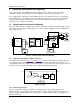
78M6610+PSU Data Sheet 4.1.1 Command-Response Protocol Description In this protocol, the host is the master and must initiate communications. The master should first select the device that needs to communicate with, then set the device’s register address pointer and finally performing the read or write operations. The sequence of operation is shown in the following diagram.
78M6610+PSU Data Sheet Register Address Pointer Selection The following message sets the address pointer to the register (or set of registers) to read or write: PAYLOAD 0xA3 Command Register Address (2 Bytes) The 78M6610+PSU replies with an acknowledge message. Read Command It is possible to read data from the 78M6610+PSU using the 0xE command. To read 0 to 15 bytes, the command byte is completed with the number of bytes to read.
78M6610+PSU Data Sheet Table 4-1 lists the commands that are supported by the 78M6610+PSU.
78M6610+PSU Data Sheet 4.1.2 Auto-Reported Data By default, the 78M6610+PSU automatically reports a set of data at the completion of each accumulation interval. This mode is used in systems where the host will not have to poll the 78M6610+PSU for data but it receives automatically data updated at the accumulation interval rate. Table 4-3 shows the default autoreported data format.
78M6610+PSU Data Sheet 4.2 SPI Interface The Maxim device operates as a SPI slave. The host is expected to instigate and control all transactions.
78M6610+PSU Data Sheet Single Word SPI Reads The device supplies direct read access to the device RAM memory. To read the RAM the master device must send a read command to the slave device and then clock out the resulting read data. SSB must be kept active low for the entire read transaction (command and response). SCK may be interrupted as long as SSB remains low. ADDR[5:0] is filled with the word address of the read transaction. RAM data contents are transmitted most significant byte first.
78M6610+PSU Data Sheet Single Word SPI Writes The device supplies direct write access to the device RAM memory. To write the RAM the master device must send a write command to the slave device and then clock out the write data. SSB must be kept active low for the entire write transaction (command and data). SCK may be interrupted as long as SSB remains low. ADDR[5:0] is filled with the word address of the write transaction. RAM data contents are transmitted most significant byte first.
78M6610+PSU Data Sheet I2C Interface 4.3 2 The 78M6610+PSU has an I C interface available at the SDAI, SDAO, and SCL pins. The interface 2 supports I C slave mode with a 7-bit address and operates at a data rate up to 400kHz. Figure 4-5 shows two possible configurations. Configuration A is the standard configuration. The double pin for SDA allows the isolated configuration B.
78M6610+PSU Data Sheet Bus Characteristics • A data transfer may be initiated only when the bus is not busy. • During data transfer, the data line must remain stable whenever the clock line is HIGH. Changes in the data line while the clock line is HIGH will be interpreted as a START or STOP condition. Bus Conditions: • Bus not Busy (I): Both data and clock lines are HIGH indicating an Idle Condition.
78M6610+PSU Data Sheet Write Operations Following the START (S) condition from the master, the device address (7-bits) and the R/W bit (logic low for write) are clocked onto the bus by the master. This indicates to the addressed slave receiver that the register address will follow after it has generated an acknowledge bit (A) during the ninth clock cycle. Therefore, the next byte transmitted by the master is the register address and will be written into the address pointer of the 78M6610+PSU.
78M6610+PSU Data Sheet If the register address pointer has not been set by previous operations, it is necessary to set it issuing a command as follows: S S 0 Device Address Register Address (n) P 0 1 2 3 4 5 6 7 0 1 2 3 4 5 6 A S C T K O P A C K S T A R T Random Read: random read operations allow the master to access any register in a random manner. To perform this operation, the register address must be set as part of the write operation.
78M6610+PSU Data Sheet 5 Electrical Specifications 5.1 Absolute Maximum Ratings Supplies and Ground Pins: V3P3D, V3P3A -0.5V to 4.6V GNDD, GNDA -0.5V to +0.5V Analog Input Pins: -10mA to +10mA -0.5V to (V3P3 + 0.5V) AVN, AVP, AIN, AIP, ATEMP1, ATEMP2 Oscillator Pins: -10mA to +10mA -0.5V to +3.0V XIN, XOUT Digital Pins: IFCONFIG, ACFAULT, ADDR1, SSB/DIR/SCL, ACCRIT;SDO/TX/SDAo, SDI/RX/SDAi, ADDR0, RELAYCTRL, MP0, MP1, RESET -30mA to +30mA, -0.5V to (V3P3D+ 0.
78M6610+PSU Data Sheet 5.4 Performance Specifications Note that production tests are performed at room temperature. 5.4.1 Input Logic Levels Parameter Condition Min Typ Max Unit Digital high-level input voltage, VIH 2 – – V Digital low-level input voltage, VIL – – 0.8 V Min Typ Max Unit ILOAD = 1 mA V3P3 –0.4 – – V ILOAD = 10 mA V3P30.6 – – V ILOAD = 1 mA 0 – 0.4 V ILOAD = 10 mA – – 0.5 V Condition Min Typ Max Unit – 8.1 10.3 mA Min Typ 5.4.
78M6610+PSU Data Sheet 5.4.6 ADC Converter, V3P3 Referenced LSB values do not include the 9-bit left shift at EMP input. Parameter Condition Usable Input Range (Vin-V3P3) Min Typ Max Unit -250 – 250 mV peak – -85 Vin=65Hz, THD (First 10 harmonics) 64kpts FFT, BlackmanHarris window 1 kΩ 1.7 – Ω/°C – 50 ppm/% 10 mV Vin=65Hz 30 – Temperature coefficient of Input Impedance Vin=65Hz – ADC Gain Error vs %Power Supply Variation 10 6 ∆Nout PK 357 nV / VIN 100 ∆V 3P3 A / 3.
78M6610+PSU Data Sheet 5.5 Timing Specifications 5.5.1 RESET Parameter Condition Min Reset pulse fall time Max Unit 1 – µs 1 1 – – 5 – µs Min Typ Max Unit 1 – – µs tSPILead Enable lead time 15 – – ns tSPILag Enable lag time 0 – – ns tSPIW SCK pulse width: High Low 250 250 – – ns ns – 2 1 – – 0 1 – ns – 25 ns Reset pulse width 1 Typ Guaranteed by design, not subject to test. 5.5.
78M6610+PSU Data Sheet 2 5.5.
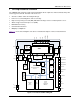
78M6610+PSU Data Sheet 6 Packaging AIN AIP V3P3A AVN AVP 24-Pin QFN Pinout ATEMP1 24 23 22 21 20 19 RESET ATEMP2 1 18 GNDA 2 17 MP0 IFCONFIG 3 16 MP1 ACFAULT 4 15 RELAYCTRL 14 SCK/ADDR0 13 SDI/RX/SDAi (Top) ACCRIT 7 8 9 10 11 12 SDO/TX/SDAo 6 GNDD SSB/DIR/SCL XOUT 5 XIN ADDR1 78M6610+PSU (24-Pin) V3P3D 6.
78M6610+PSU Data Sheet 6.
78M6610+PSU Data Sheet 6.3 Package Outline PACAKGE TYPE PACAKGE CODE OUTLINE NO. LAND PATTERN NO.
78M6610+PSU Data Sheet TSSOP-16 Package Rev 3 63
78M6610+PSU Data Sheet 7 Ordering Information Part Package QFN-24 78M6610+PSU TSSOP-16 8 Option Ordering Number Bulk 78M6610+PSU/B00 Tape & Reel 78M6610+PSU/B00T Bulk 78M6610+PSU/C00 Tape & Reel 78M6610+PSU/C00T IC Marking EMP Contact Information For more information about the 78M6610+PSU or other Maxim Integrated products, contact technical support at www.maximintegrated.com/support.
DS_6610_096 78M6610+PSU Data Sheet Revision History REVISION NUMBER REVISION DATE 0 7/12 Initial release 1 2/13 Revised pin description, RC Oscillator Specification, X+Y capacitor calibration, and accumulation interval description 7, 12, 13, 19, 20, 40, 45, 54, 55, 58, 59 2 4/14 Updated the Command Register and SPI Interface sections; revised the SSI byte count description; updated related tables 20, 21, 38, 39, 40, 48, 50 3 8/14 Updated Storage Temperature parameter on the Electrical Chara