
Datasheet
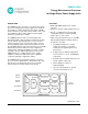


78M6610+PSU Data Sheet
Table of Contents
1 On-Chip Resources Overview ........................................................................................................... 5
1.1 Clock Management ...................................................................................................................... 6
1.2 Power-On Reset, WD Timer, and Reset Circuitry ....................................................................... 7
1.3 Analog Front-End and Conversion .............................................................................................. 8
1.4 24-Bit Energy Measurement Processor (EMP)............................................................................ 8
1.5 Flash and RAM ............................................................................................................................ 8
1.6 Communication Peripherals ......................................................................................................... 8
1.7 Multi-Purpose Digital I/O Pins ...................................................................................................... 9
1.8 Alarm Pins (ACFAULT, ACCRIT) ................................................................................................ 9
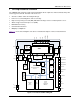
2 Functional Description and Operation ........................................................................................... 10
2.1 Voltage and Current Inputs Conditioning ................................................................................... 10
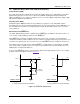
2.1.1 High Pass Filters (HPF) and Offset Correction .............................................................. 10
2.1.2 Phase Compensation .................................................................................................... 10
2.2 Current and Voltage RMS Calculations ..................................................................................... 11
2.3 Power Calculations and Power Factor ....................................................................................... 12
2.3.1 Active Power Calculation ............................................................................................... 12
2.3.2 Apparent Power ............................................................................................................. 12
2.3.3 Power Factor.................................................................................................................. 12
2.3.4 Reactive Power .............................................................................................................. 12
2.4 Fundamental and Harmonics Calculations ................................................................................ 13
2.5 Accumulation Interval ................................................................................................................. 13
2.6 Zero-Crossing Detection ............................................................................................................ 14
2.7 Alarms ........................................................................................................................................ 14
2.8 Voltage and Current Min/Max and Peak Tracking ..................................................................... 15
2.8.1 Voltage and Current Min/Max Tracking ......................................................................... 15
2.8.2 Voltage and Current Peak Tracking .............................................................................. 15
2.9 X+Y Capacitor Current and I/R Voltage Drop Compensation ................................................... 15
2.9.1 X+Y Capacitor Compensation ....................................................................................... 15
2.9.2 I/R Voltage Drop Compensation .................................................................................... 16
2.10 External Temperature Monitor ................................................................................................... 16
2.11 Voltage Sag and Surge Detection ............................................................................................. 17
2.12 Relay Control ............................................................................................................................. 18
2.12.1 Autonomous Mode ......................................................................................................... 18
2.12.2 Slave Mode .................................................................................................................... 18
2.12.3 Activation Delay ............................................................................................................. 18
2.13 On-Chip Calibration Routines .................................................................................................... 20
2.13.1 Voltage and Current Gain Calibration ............................................................................ 20
2.13.2 Offset Calibration ........................................................................................................... 20
2.13.3 X+Y Capacitor and R Compensation Coefficient Calibration ........................................ 20
2.13.4 On-Chip Temperature Calibration.................................................................................. 21
2.13.5 External Temperature Calibration .................................................................................. 21
3 Data Access and Configurability ..................................................................................................... 22
3.1 Register Descriptions ................................................................................................................. 22
3.2 Scaling Registers (Iscale, Vscale, Pscale, Tscale, Fscale) ....................................................... 24
3.3 Output Registers ........................................................................................................................ 25
3.4 Input Registers (Setup and Calibration) ..................................................................................... 27
3.5 Relay Configuration ................................................................................................................... 29
3.6 DIOState Register ...................................................................................................................... 30
3.7 Alarms and Alarms Configuration Registers .............................................................................. 31
3.7.1 Alarms Status Register (address 0x30) ......................................................................... 31
3.7.2 AlarmSticky Register (address 0x54) ............................................................................ 32
3.7.3 AlarmMask1 (address 0x09) and AlarmMask2 (address 0x51) .................................... 33
3.7.4 AlarmSet Register (address 0x0C) ................................................................................ 34
3.7.5 AlarmReset Register (address 0x0F) ............................................................................ 35
3.7.6 Alarms Configuration Registers (Thresholds and Hold-Off Time) ................................. 36
2 Rev 3