
Datasheet
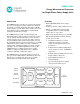


78M6610+PSU Data Sheet
3.7.7 Alarm Counter Registers ............................................................................................... 37
3.8 Command Register .................................................................................................................... 38
3.8.1 General Settings ............................................................................................................ 38
3.8.2 No Action (0x00xxxx) ..................................................................................................... 38
3.8.3 Save to Flash Command (0xACC2xx) ........................................................................... 39
3.8.4 Clear Flash Storage 0 Command (0xACC0xx) .............................................................. 39
3.8.5 Clear Flash Storage 1 Command (0xACC1xx) .............................................................. 39
3.8.6 Calibration Command (0xCAxxxx)................................................................................. 40
4 Serial Interfaces ................................................................................................................................ 41
4.1 UART Interface .......................................................................................................................... 43
4.1.1 Command-Response Protocol Description ................................................................... 44
4.1.2 Auto-Reported Data ....................................................................................................... 47
4.2 SPI Interface .............................................................................................................................. 48
4.3 I
2
C Interface ............................................................................................................................... 51
5 Electrical Specifications ................................................................................................................... 55
5.1 Absolute Maximum Ratings ....................................................................................................... 55
5.2 Recommended External Components ....................................................................................... 55
5.3 Recommended Operating Conditions ........................................................................................ 55
5.4 Performance Specifications ....................................................................................................... 56
5.4.1 Input Logic Levels .......................................................................................................... 56
5.4.2 Output Logic Levels ....................................................................................................... 56
5.4.3 Supply Current ............................................................................................................... 56
5.4.4 Crystal Oscillator ............................................................................................................ 56
5.4.5 Internal RC Oscillator ..................................................................................................... 56
5.4.6 ADC Converter, V
3P3
Referenced .................................................................................. 57
5.5 Timing Specifications ................................................................................................................. 58
5.5.1 RESET ........................................................................................................................... 58
5.5.2 SPI Slave Port................................................................................................................ 58
5.5.3 I
2
C Slave Port ................................................................................................................ 59
6 Packaging .......................................................................................................................................... 60
6.1 24-Pin QFN Pinout ..................................................................................................................... 60
6.2 16-Pin TSSOP Pinout ................................................................................................................ 61
6.3 Package Outline ......................................................................................................................... 62
7 Ordering Information ........................................................................................................................ 64
8 Contact Information .......................................................................................................................... 64
Revision History ........................................................................................................................................ 65
List of Figures
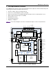
Figure 1-1: IC Functional Block Diagram ......................................................................................... 5
Figure 1-2: XTAL Connection .......................................................................................................... 6
Figure 1-3: RESET Pin Connections ............................................................................................... 7
Figure 2-1: Analog Input Signal Conditioning ................................................................................ 10
Figure 2-2: HPF .............................................................................................................................. 10
Figure 2-3: RMS Calculations ........................................................................................................ 11
Figure 2-4: Power (Active, Reactive, and Apparent) and Power Factor Calculation ..................... 12
Figure 2-5: Voltage and Current Fundamental and Harmonic Calculations .................................. 13
Figure 2-6: Typical Measurement Location in Power Supplies...................................................... 15
Figure 2-7: External Temperature Monitor ..................................................................................... 16
Figure 2-8: Typical Sag Event ........................................................................................................ 17
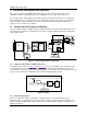
Figure 2-9: Relay Control for In-rush Current Limitation Circuitry.................................................. 18
Figure 2-10: Relay Control ............................................................................................................. 19
Figure 2-11: Typical Calibration Setup ........................................................................................... 21
Figure 4-1: UART Connections on a RS-485 Bus ......................................................................... 43
Rev 3 3