
Datasheet


78M6610+PSU Data Sheet
Figure 4-2: Signal Timing on the SPI Bus ...................................................................................... 48
Figure 4-3: Single Word Read Access Timing ............................................................................... 49
Figure 4-4: Single Word Write Access Timing ............................................................................... 50
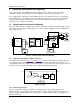
Figure 4-5: I
2
C Bus Connection in Standard (A) and Isolated (B) Configuration ........................... 51
Figure 4-6: I
2
C Bus 3-byte Data Write ........................................................................................... 53
Figure 4-7: I
2
C Bus Multiple Sequential Register Write ................................................................. 53
Figure 5-1: SPI Slave Port Timing ................................................................................................. 58
Figure 5-2: I
2
C (Slave) Port Timing ................................................................................................ 59
List of Tables
Table 1-1: Alarm Pins Functional Description .................................................................................. 9
Table 2-1: Relay Configuration Register and Sequence Delay Register ....................................... 19
Table 3-1: Data Type Description .................................................................................................. 23
Table 3-2: Registers with Scalable Values .................................................................................... 24
Table 3-3: Output Registers ........................................................................................................... 25
Table 3-4: High-Rate Result Registers .......................................................................................... 26
Table 3-5: Input Registers .............................................................................................................. 27
Table 3-6: Relay Configuration Registers ...................................................................................... 29
Table 3-7: DIOState Register ......................................................................................................... 30
Table 3-8: Alarms Register and Corresponding Configuration Registers ...................................... 31
Table 3-9: AlarmSticky Register Bits Assignment ......................................................................... 32
Table 3-10: AlarmMask1 and AlarmMask2 Registers Bits Assignment ........................................ 33
Table 3-11: AlarmSet Register Bit Assignments ............................................................................ 34
Table 3-12: AlarmReset Registers Bit Assignments ...................................................................... 35
Table 3-13: Alarms Threshold Registers ....................................................................................... 36
Table 3-14: Alarms Hold-Off Timers Registers .............................................................................. 37
Table 3-15: Alarms Counter Registers ........................................................................................... 37
Table 3-16: General Settings Command Bits ................................................................................ 38
Table 3-17. No Action Command Bits ............................................................................................ 38
Table 3-18. Save to Flash Command Bits ..................................................................................... 39
Table 3-19. Clear Flash Storage 0 Command Bits ........................................................................ 39
Table 3-20. Clear Flash Storage 1 Command Bits ........................................................................ 39
Table 3-21. Calibration Command Bits .......................................................................................... 40
Table 4-1: Host Commands ........................................................................................................... 46
Table 4-2: Slave Reply Codes ....................................................................................................... 46
Table 4-3: Default Measurements .................................................................................................. 47
Table 4-4. Single Word SPI Read Command (SDI) ....................................................................... 49
Table 4-5. Single Word SPI Read Response (SDO) ..................................................................... 49
Table 4-6. Single Word SPI Write Command and Data (SDI) ....................................................... 50
Table 5-1: I
2
C Slave Port Timing
2
.................................................................................................. 59
4 Rev 3