78M6610+PSU Hardware Design Guidelines APPLICATION NOTE AN_6610_107 July 2012 1 Introduction This application note describes hardware and system design guidelines for incorporating precision power monitoring of better than 1% accuracy into AC/DC power supplies using the 78M6610+PSU. For real-time embedded measurement of the AC input power in a power supply, there are three possible sensor locations: 1. Measuring behind the EMI filtering circuit (recommended).
78M6610+PSU Hardware Design Guidelines AN_6610_107 2 Recommended Configuration Resistive current shunts and voltage dividers are commonly used to meet system limitations on size and cost. When using a shunt current sensor, the measurement IC and its power domain are directly connected to AC mains. In this case, the 78M6610+PSU measurement device is typically powered through an auxiliary winding of the SMPS transformer (generally the stand-by channel).
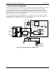
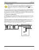
AN_6610_107 2.1 78M6610+PSU Hardware Design Guidelines Sensor Connections The basic connections for a shunt-based system are represented below. LINE 1M V3P3 100nF 1M 1000pF 100nF 750 AVP V3P3 ATEMP AVN NTC LOAD INPUT NEUTRAL 1000pF 100nF 1000pF V3P3 AIP 750 750 100nF AIN 78M6610+PSU Shunt Figure 2: Basic Connection Diagram on Shunt-Based Systems The 78M6610+PSU makes use of a single 3.
78M6610+PSU Hardware Design Guidelines 2.1.1 AN_6610_107 Line Voltage Resistor Divider Selection The input AC line voltage is scaled down to match the 78M6610+PSU’s ADC input signal range of ±176.78 mVrms (+/-250mV pk-pk). To support most 2-wire AC voltages with enough overhead for surges, a peak RMS voltage of 471 VAC is recommended. Using the circuit in the previous figure, the line voltage is scaled down as follows: 𝑉𝐴𝐷𝐶 = 𝑉𝐿𝐼𝑁𝐸 ∗ 750 = 𝑉𝐿𝐼𝑁𝐸 ∗ 3.
AN_6610_107 2.1.2 78M6610+PSU Hardware Design Guidelines Shunt Resistor Selection The value of the shunt to be used is a tradeoff between a higher shunt value that utilizes the full analog sensor input range of the IC and the lowest possible value that minimizes the power loss in the shunt. For best utilization of the device’s input range (+/-250 mVpp) and performance at lower currents, a larger shunt value that supports the maximum input current without clipping peak currents should be used.
78M6610+PSU Hardware Design Guidelines 2.2 AN_6610_107 Safety Precautions With V3P3 directly connected to NEUTRAL, the 78M6610+PSU’s Ground signal can be -3.3 V below earth ground. Any external test equipment attached to the 78M6610+PSU will be subject to this -3.3 V ground reference disparity. External test equipment must be disconnected from earth ground to avoid equipment damage due to this ground reference disparity. A more serious safety issue may arise due to mis-wiring of the AC circuit.
AN_6610_107 78M6610+PSU Hardware Design Guidelines 3 Alternate Configuration Voltage and current sensors can alternatively be located right at the AC inlet in front of the EMI filters if using a current transformer (CT). In this configuration, the measurement device is powered using the same auxiliary winding from the standby channel, but with a high impedance path between 78M6610+PSU circuitry and AC mains.
78M6610+PSU Hardware Design Guidelines 3.1 AN_6610_107 Current Transformer Selection The consideration for selecting a current transformer should include measurement accuracy, line frequency (and harmonics), current range and the CT’s turns ratio. The load current range should also be considered. Subjecting a current transformer to load currents above the manufacturer’s rated current specification may saturate the CT and cause winding failures due to excessive temperature rise.
AN_6610_107 78M6610+PSU Hardware Design Guidelines 4 Device Configuration The following section covers the rest of the hardware interfaces found on the 78M6610+PSU. 4.1 VDC Supply (V3P3D, V3P3A) and Decoupling The 78M6610+PSU requires a single 3.3VDC supply. In order to minimize the effect of digital output switching on the analog circuitry, the 78M6610+PSU has separate supply pins for analog (V3P3A/GNDA) and digital circuitry (V3P3D/GNDD).
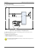
78M6610+PSU Hardware Design Guidelines AN_6610_107 The basic power supply filter connections are shown in Figure 6, showing also the required decoupling capacitors. 3.3 VDC bypassing incorporates the combination of three different capacitor values. A 1000 pF in parallel with a 0.1 µF ceramic capacitor must be placed as close as possible to the 78M6610+PSU V3P3A pin. Place the 1000 pF capacitor closest to the V3P3A pin of the 78M6610+PSU.
AN_6610_107 4.2 78M6610+PSU Hardware Design Guidelines Clock Circuitry The 78M6610+PSU can utilize an external 20.000 MHz crystal for optimum performance. The circuitry includes two ceramic capacitors. The selected crystal must have a specified 18 pF load capacitance. The oscillator is specifically designed for these types of crystals which have high impedance and limited power handling capability. The oscillator design minimizes power dissipation.
78M6610+PSU Hardware Design Guidelines 4.3 AN_6610_107 Reset Circuitry The 78M6610+PSU employs an active low Reset input pin. Figure 8 shows the external circuit configuration using a pushbutton switch to generate the reset signal. If an external reset is not required, connect the Reset pin to V3P3. An external reset is typically only used during the development phase of a project. The RESET pin can be tied high for the production version of the PCB.
AN_6610_107 4.4 78M6610+PSU Hardware Design Guidelines Connecting 5 V Devices All digital input pins (DIO pins) of the 78M6610+PSU are 5 V tolerant allowing connection to external 5 V devices. I/O pins configured as inputs do not require current-limiting resistors when they are connected to external 5 V devices. 4.
78M6610+PSU Hardware Design Guidelines AN_6610_107 5 Printed Circuit Board Layout Guidelines The 78M6610+PSU minimizes the external component count and reduces the complexity of the printed circuit board layout design. However, some elements of the board design require consideration for optimum measurement accuracy and reliability.
AN_6610_107 5.2 78M6610+PSU Hardware Design Guidelines Crystal Oscillator Components The 78M6610+PSU Evaluation Board has the crystal and its two load capacitors located on the bottom layer. Place a GND trace between the two terminals of the crystal to minimize oscillator startup problems. GND Via Crystal GND Isolator GND Via Figure 10: Crystal Y1 and Capacitors C8/ C11 The 78M6610+PSU can operate without an external crystal. Attach the XOUT pin to GND when the external crystal is not used. Rev.
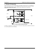
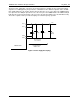
78M6610+PSU Hardware Design Guidelines 5.3 AN_6610_107 LINE Voltage Resistor Network The LINE voltage resistor network can be split between a 78M6610+PSU (daughter) board and the host board. The 750 Ω termination resistor and anti-aliasing capacitors should be placed near the 78M6610+PSU’s analog input pin. Termination Resistor 78M6610+PSU Anti-Aliasing Capacitors Figure 11: LINE Voltage Filter Network The high voltage 1 MΩ resistors can be placed remotely on the host board.
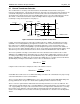
AN_6610_107 5.4 78M6610+PSU Hardware Design Guidelines Shunt Current Sensor The current shunt network can also be split between the 78M6610+PSU (daughter) board and the host board. The 750 Ω termination resistors and anti-aliasing capacitors should be placed near the 78M6610+PSU’s analog input pins. 78M6610+PSU Termination Resistors Anti-Aliasing Capacitors Figure 13: AIP and AIN Filter Network The resistive current shunt can be placed remotely on the host board.
78M6610+PSU Hardware Design Guidelines 5.6 AN_6610_107 V3P3 Decoupling Capacitors Place the V3P3 decoupling capacitors close to the 3.3V regulator and 78M6610+PSU. Provide adequate V3P3 copper plane from the voltage regulator and decoupling capacitors to the V3P3D and V3P3D pins of the 78M6610+PSU. Two separate V3P3A and V3P3D planes are recommended, but they should be electrically connected via either a zero ohm resistor or inductor if needed. Figure 15: V3P3 C3, C4, C5 Decoupling Capacitors 5.
AN_6610_107 78M6610+PSU Hardware Design Guidelines 6 Revision History Revision Date Description 0 7/27/2012 First publication. Maxim cannot assume responsibility for use of any circuitry other than circuitry entirely embodied in a Maxim product. No circuit patent licenses are implied. Maxim reserves the right to change the circuitry and specifications without notice at any time. Maxim Integrated Products, Inc.