
Datasheet
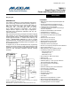


DS_6612_001 78M6612 Data Sheet
Rev 2 3
4.3 Recommended Operating Conditions .................................................................................... 29
4.4 Performance Specifications ................................................................................................... 30
4.4.1 Input Logic Levels ..................................................................................................... 30
4.4.2 Output Logic Levels ................................................................................................... 30
4.4.3 Power-Fault Comparator ........................................................................................... 30
4.4.4 Battery Monitor .......................................................................................................... 31
4.4.5 Supply Current .......................................................................................................... 31
4.4.6 V3P3D Switch ........................................................................................................... 31
4.4.7 2.5V Voltage Regulator ............................................................................................. 32
4.4.8 Low Power Voltage Regulator ................................................................................... 32
4.4.9 Crystal Oscillator ....................................................................................................... 32
4.4.10 VREF, VBIAS ............................................................................................................ 33
4.4.11 LCD Drivers .............................................................................................................. 33
4.4.12 ADC Converter, V3P3A Referenced .......................................................................... 34
4.4.13 UART1 Interface........................................................................................................ 34
4.4.14 Temperature Sensor.................................................................................................. 34
4.5 Timing Specifications ............................................................................................................ 35
4.5.1 RAM and Flash Memory ............................................................................................ 35
4.5.2 Flash Memory Timing ................................................................................................ 35
4.5.3 EEPROM Interface .................................................................................................... 35
4.5.4 RESET and V1 .......................................................................................................... 35
4.5.5 RTC .......................................................................................................................... 35
5 Packaging .................................................................................................................................... 36
5.1 64-Pin LQFP Package .......................................................................................................... 36
5.1.1 Pinout........................................................................................................................ 36
5.1.2 Package Outline (LQFP 64) ....................................................................................... 37
5.1.3 Recommended PCB Land Pattern for the LQFP-64 Package..................................... 38
5.2 68-Pin QFN Package ............................................................................................................ 39
5.2.1 Pinout........................................................................................................................ 39
5.2.2 Package Outline ........................................................................................................ 40
5.2.3 Recommended PCB Land Pattern for the QFN-68 Package ...................................... 41
6 Pin Descriptions .......................................................................................................................... 42
6.1 Power/Ground Pins ............................................................................................................... 42
6.2 Analog Pins........................................................................................................................... 42
6.3 Digital Pins ............................................................................................................................ 43
7 I/O Equivalent Circuits ................................................................................................................. 44
8 Ordering Information ................................................................................................................... 45
9 Contact Information ..................................................................................................................... 45
Revision History .................................................................................................................................. 46