
Datasheet
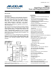


DS_6612_001 78M6612 Data Sheet
Rev 2 5
Tables
Table 1: Inputs Selected in Regular and Alternate Multiplexer Cycles ....................................................... 8
Table 2: Data/Direction Registers and Internal Resources for DIO Pin Groups ....................................... 14
Table 3: DIO_DIR Control Bit ................................................................................................................. 15
Table 4: Selectable Controls using the DIO_DIR Bits ............................................................................. 16
Table 5: Absolute Maximum Ratings ...................................................................................................... 28
Table 6: Recommended External Components ...................................................................................... 29
Table 7: Recommended Operation Conditions ....................................................................................... 29
Table 8: Input Logic Levels .................................................................................................................... 30
Table 9: Output Logic Levels ................................................................................................................. 30
Table 10: Power-Fault Comparator Performance Specifications ............................................................. 30
Table 11: Power-Fault Comparator Performance Specifications (BME=1) .............................................. 31
Table 12: Supply Current Performance Specifications ............................................................................ 31
Table 13: V3P3D Switch Performance Specifications ............................................................................. 31
Table 14: 2.5 V Voltage Regulator Performance Specifications .............................................................. 32
Table 15: Low-Power Voltage Regulator Performance Specifications ..................................................... 32
Table 16: Crystal Oscillator Performance Specifications ......................................................................... 32
Table 17: VREF, VBIAS Performance Specifications.............................................................................. 33
Table 18: LCD Drivers Performance Specifications ................................................................................ 33
Table 19: ADC Converter Performance Specifications ........................................................................... 34
Table 20: UART1 Interface Performance Specifications ......................................................................... 34
Table 21: Temperature Sensor Performance Specifications ................................................................... 34
Table 22: RAM and Flash Memory Specifications .................................................................................. 35
Table 23: Flash Memory Timing Specifications ...................................................................................... 35
Table 24: EEPROM Interface Timing ..................................................................................................... 35
Table 25: RESET and V1 Timing ........................................................................................................... 35
Table 26: RTC Range ............................................................................................................................ 35
Table 27: Power/Ground Pins ................................................................................................................ 42
Table 28: Analog Pins ............................................................................................................................ 42