
Datasheet


DG201A/DG211
Quad SPST CMOS Analog Switches
6 _______________________________________________________________________________________
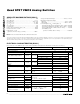
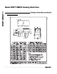
R
DS(ON)
AT ANALOG SIGNAL LEVEL
POWER SUPPLIES
-5V +5V -10V +10V -15V +15V
±5V 350Ω 380Ω ————
±10V — — 165Ω 250Ω ——
±15V — — 125Ω 160Ω 135Ω 155Ω
Typical R
DS(ON)
vs. Power Supplies for Maxim’s DG201A, and DG211
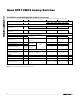
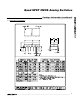
Protecting Against Fault
Conditions
Fault conditions occur when power supplies are turned
off when input signals are still present, or when over-
voltages occur at the inputs during normal operation. In
either case, source-to-body diodes can be forward
biased and conduct current from the signal source. If
this current is required to be kept to low (µA) levels
then the addition of external protection diodes is rec-
ommended.
To provide protection for overvoltages up to 20V above
the supplies, a 1N4001 or 1N914 type diode should be
placed in series with the positive and negative supplies
as shown in Figure 2. The addition of these diodes will
reduce the analog signal range to 1V below the posi-
tive supply and 1V above the negative supply.
16
15
14
13
12
11
10
9
1
2
3
4
5
6
7
8
DG201A
DG211
IN4001
-15V
IN4001
+15V
Figure 2. Protection against Fault Conditions
LOGIC "0" - SW ON
3V
V
S
0
LOGIC
INPUT
t
f
< 20ns
t
r
< 20ns
SWITCH
INPUT
SWITCH
OUTPUT
50%
0
V
0
0.9
t
ON
V
0
V
0
0.9
0.1
t
off1
t
off2
Ω
SWITCH
INPUT
S
1
V
S
= +2V
IN
1
LOGIC
INPUT
GND
0
V-
-15V
+15V
V
+
D
1
R
L
1kΩ
C
L
35pF
V
0
SWITCH
OUTPUT
(REPEAT TEST FOR IN
2
, IN
3
,
AND IN
4
)
V
0
= V
S
R
L
R
L
+ R
DS(ON)
TOP VIEW
16 15 14 13
5
1
2
3
4
12
11
10
9
678
S1
V-
GND
S4
S2
V+
N.C.
S3
D1 IN1 IN2 D2
D4 IN4 IN3 D3
DG201A
DG211
QFN*
Pin Configurations (continued)
Figure 1. Switching Time