
Datasheet
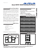

DG201A/DG211
Quad SPST CMOS Analog Switches
2 _______________________________________________________________________________________
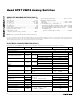
ABSOLUTE MAXIMUM RATINGS (DG211)
ELECTRICAL CHARACTERISTICS (DG211)
(V+ = +15V, V- = -15V, GND = 0, T
A
= +25°C, unless otherwise noted.) (For more information on TYP values see Note 2.)
Stresses beyond those listed under “Absolute Maximum Ratings” may cause permanent damage to the device. These are stress ratings only, and functional
operation of the device at these or any other conditions beyond those indicated in the operational sections of the specifications is not implied. Exposure to
absolute maximum rating conditions for extended periods may affect device reliability.
V+ to V-………………………………….............……………….44V
V
IN
to Ground…………………………..................…. ……...V-, V+
V
L
to Ground………....................……………………….-0.3V, 25V
V
S
or V
D
to V+……...........................………………………0, -40V
V
S
or V
D
to V-……………........................…………………..0, 40V
V+ to Ground…………………...................................………...25V
V- to Ground…………………………………….................…...-25V
Current, Any Terminal Except S or D……….............……...30mA
Continuous Current, S or D……………………..............…...20mA
Peak Current, S or D
(pulsed at 1ms 10% duty cycle max)…..........................70mA
Storage Temperature Range……………..……..-65°C to +125°C
Operating Temperature Range
DG211C................................……………...……...0°C to +70°C
DG211D/E .........................……………...……...-40°C to +85°C
Power Dissipation (T
A
= +70°C) (Note 1)
16-Pin Plastic Dip (derate 10.5mW/°C above +70°C) ..842mW
16-Pin Narrow SO (derate 8.3mW/°C above+70°C). ....696mW
16-Pin TSSOP (derate 9.4mW/°C above +70°C) ..........755mW
16-Pin QFN (5
✕ 5)
(derate 19.2mW/°C above +70°C).........................1538mW
PARAMETER
SYMBOL
CONDITIONS MIN TYP
MAX
UNITS
SWITCH
Analog Signal Range
V
ANALOG
-15 15 V
Drain-Source ON-Resistance
R
DS
(
ON
)
V
D
= ±10V, V
IN
= 0.8V, I
S
= 1mA 115 175 Ω
V
S
= 14V, V
D
= -14V 0.01 5.0
Source OFF-Leakage Current
I
S
(
OFF
)
V
IN
= 2.4V
V
S
= -14V, V
D
= 14V -5.0 -0.02
V
S
= 14V, V
D
= -14V 0.01 5.0
Drain OFF-Leakage Current
I
D
(
OFF
)
V
IN
= 2.4V
V
S
= -14V, V
D
= 14V -5.0 -0.02
V
S
= V
D
= -14V 0.1 5.0
Drain ON-Leakage Current
(Note 3)
I
D (ON)
V
IN
= 0.8V
V
S
= V
D
= -14V -5.0 -0.15
nA
INPUT
V
IN
= 2.4V -1.0
-0.0004
Input Current with Input Voltage
High
I
INH
V
IN
= 15V
0.003
1.0
Input Current with Input Voltage
Low
I
INL
V
IN
= 0 -1.0
-0.0004
µA
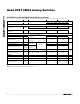
DYNAMIC
Turn-ON Time t
ON
460
1000
t
OFF1
360 500
Turn-OFF Time
t
OFF2
See Switching Time
Test Circuit
V
S
= 2V, R
L
= 1kΩ, C
L
= 35pF
450
ns
Source OFF-Capacitance
C
S
(
OFF
)
V
S
= 0, V
IN
= 5V, f = 1MHz 5
Drain OFF-Capacitance
C
D
(
OFF
)
V
D
= 0, V
IN
= 5V, f = 1MHz 5
Channel ON-Capacitance
C
D + S
(
ON
)
V
D
= V
S
= 0, V
IN
= 0, f = 1MHz 16
pF
OFF-Isolation (Note 4) OIRR 70
Crosstalk
(Channel to Channel)
CCRR
V
IN
= 5V, R
L
= 1kΩ, C
L
= 15pF,
V
S
= 1VRMS, f = 100kHz
90
dB
Note 1: Device mounted with all leads soldered to PC board.