
Datasheet

_______________________________________________________________________________________ 5
DG201A/DG211
Quad SPST CMOS Analog Switches
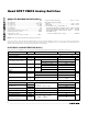
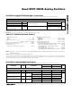
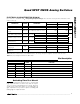
ELECTRICAL CHARACTERISTICS (DG201A)
(V+ = +15V, V- = -15V, GND = 0, T
A
= full opearting temperature range, unless otherwise noted.) (For more information on TYP
values see Note 3.)
DG201AA DG201AC, D, E
PARAMETER
SYMBOL
CONDITIONS
MIN TYP MAX MIN TYP MAX
UNITS
SWITCH
Analog Signal Range
V
ANALOG
-15 15 -15 15
V
D r ai n- S our ce ON Resi stance
( N ote 5)
R
DS
(
ON
)
V
D
= ±10V, V
IN
= 0.8V, I
S
= 1mA
250 250
Ω
V
S
= 14V, V
D
= -14V 100 100
Source OFF Leakage Current
I
S
(
OFF
)
V
IN
= 2.4V
V
S
= -14V, V
D
= 14V -100 -100
V
S
= 14V, V
D
= -14V 100 100
Drain OFF Leakage Current
I
D
(
OFF
)
V
IN
= 2.4V
V
S
= -14V, V
D
= 14V -100 -100
V
S
= -14V
200 200
Drain ON Leakage
Current (Note 6)
I
D
(
ON
)
V
IN
= 0.8V
V
D
= 14V
-200 -200
nA
INPUT
V
IN
= 2.4V
-1.0 -1.0
Input Current with Input
Voltage High
I
INH
V
IN
= 15V
1.0 1.0
Input Current with Input
Voltage Low
I
INL
V
IN
= 0
-1.0 -1.0
µA
Note 5: Electrical characteristics, such as ON-Resistance, will change when power supplies other than ±15V, are used.
Note 6: I
D (ON)
is leakage from driver into “ON” switch.
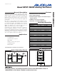
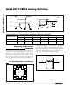
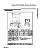
PIN
DIP/SO/TSSOP
QFN
NAME FUNCTION
1, 16, 9, 8 15, 14, 7, 6
IN1–IN4
Input
2, 15, 10, 7 16, 13, 8, 5 D1–D4 Analog Switch Drain Terminal
3, 14, 11, 6 1, 12, 9, 4 S1–S4 Analog Switch Source Terminal
42V- Negative-Supply Voltage Input
53GND Ground
12 10 N.C. No Connection
13 11 V+ Positive-Supply Voltage Input—Connected to Substrate
Pin Description
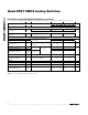
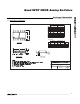
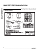
Switching Time Test Circuit
Switch output waveform shown for V
S
= constant with
logic input waveform as shown. Note that V
S
may be
+ve or -ve as per switching times test circuit. V
O
is the
steady state output with switch on. Feedthrough via
gate capacitance may result in spikes at leading and
trailing edge of output waveform.