
Datasheet
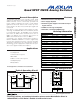


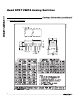

DG201A/DG211
Quad SPST CMOS Analog Switches
4 _______________________________________________________________________________________
Note 3: Typical values are for DESIGN AID ONLY, not guaranteed nor subject to production testing.
Note 4: I
D (ON)
is leakage from driver into “ON” switch.
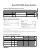
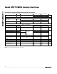
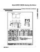
DG201AA DG201AC, D, E
PARAMETER
SYMBOL
CONDITIONS
MIN TYP MAX MIN TYP MAX
UNITS
INPUT
V
IN
= 2.4V
-1.0 -1.0
Input Current with Input
Voltage High
I
INH
V
IN
= 15V
1.0 1.0
Input Current with Input
Voltage Low
I
INL
V
IN
= 0+
-1.0 -1.0
µA
DYNAMIC
Turn-ON Time t
ON
480 600 480 600
Turn-OFF Time t
OFF1
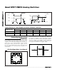
See Figure 1 Switching Time
Test Circuit
370 450 370 450
ns
Charge Injection Q
C
L
= 1000pF, V
GEN
= 0,
R
GEN
= 0
20 20
pC
Source OFF-Capacitance
C
S
(
OFF
)
55
Drain OFF-Capacitance
C
D
(
OFF
)
V
S
= 0,
V
IN
= 5V
55
Channel ON-Capacitance
C
D
(
ON
)
+ C
S
(
ON
)
V
D
= V
S
= 0,
V
IN
= 0
f = 140kHz
16 16
pF
OFF-Isolation V
IN
= 5V, Z
L
= 75Ω
70 70
Crosstalk
(Channel to Channel)
V
S
= 2.0V, f = 100kHz
90 90
dB
SUPPLY
Positive Supply Current I
+
All channels ON or OFF
0.02 0.1 0.02 0.1
mA
Negative Supply Current I
-
All channels ON or OFF
-0.1 -0.01 -0.1 -0.01
Power-Supply Range for
Continuous Operation
V
OP
±4.5 ±18 ±4.5 ±18
V
ELECTRICAL CHARACTERISTICS (DG201A) (continued)
(V+ = +15V, V- = -15V, GND = 0, T
A
= +25°C, unless otherwise noted.) (For more information on TYP values see Note 3.)