
Datasheet


_______________________________________________________________________________________ 5
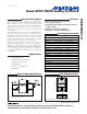
DG202/DG212
Quad SPST CMOS Analog Switches
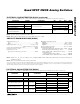
ELECTRICAL CHARACTERISTICS (DG202)
(V+ = +15V, V- = -15V, GND = 0, T
A
= full opearting temperature range, unless otherwise noted.) (For more information on TYP
values see Note 3.)
DG202A DG202C, D, E
PARAMETER
SYMBOL
CONDITIONS
MIN TYP MAX MIN TYP MAX
UNITS
SWITCH
Analog Signal Range
V
ANALOG
-15 +15 -15 +15
V
Drain-Source ON Resistance
(Note 5)
R
DS
(
ON
)
V
D
= ±10V, V
IN
= 2.4V, I
S
= 1mA
250 250
Ω
V
S
= 14V, V
D
= -14V 100 100
Source OFF-Leakage Current
I
S
(
OFF
)
V
IN
= 0.8V
V
S
= -14V, V
D
= 14V -100 -100
V
S
= 14V, V
D
= -14V 100 100
Drain OFF-Leakage Current
I
D
(
OFF
)
V
IN
= 0.8V
V
S
= -14V, V
D
= 14V -100 -100
V
S
= -14V
200 200
Drain ON-Leakage Current
(Note 6)
I
D
(
ON
)
V
IN
= 2.4V
V
D
= 14V
-200 -200
nA
INPUT
V
IN
= 2.4V
-1.0 -1.0
Input Current with Input
Voltage High
I
INH
V
IN
= 15V
1.0 1.0
Input Current with Input
Voltage Low
I
INL
V
IN
= 0
-1.0 -1.0
µA
Note 5: Electrical characteristics, such as On-Resistance, will change when power supplies other than ±15V, are used.
Note 6: I
D (ON)
is leakage from driver into “ON” switch.
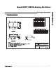
PIN
DIP/SO/TSSOP
QFN/TQFN
NAME FUNCTION
1, 16, 9, 8 15, 14, 7, 6
IN1–IN4
Input
2, 15, 10, 7 16, 13, 8, 5 D1–D4 Analog Switch Drain Terminal
3, 14, 11, 6 1, 12, 9, 4 S1–S4 Analog Switch Source Terminal
42V- Negative-Supply Voltage Input
53GND Ground
12 10 N.C. No Connection
13 11 V+ Positive-Supply Voltage Input—Connected to Substrate
—EPEPExposed Pad. Connect exposed pad to V+ or leave EP unconnected.
Pin Description
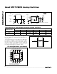
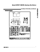
Switching Time Test Circuit
Switch output waveform shown for V
S
= constant with
logic input waveform as shown. Note that V
S
may be
+ve or -ve as per switching times test circuit. V
O
is the
steady state output with switch on. Feedthrough via
gate capacitance may result in spikes at leading and
trailing edge of output waveform.
Protecting Against Fault
Conditions
Fault conditions occur when power supplies are turned
off when input signals are still present, or when over-
voltages occur at the inputs during normal operation. In
either case, source-to-body diodes can be forward
biased and conduct current from the signal source. If