
Datasheet


DS1023
4 of 16
For highest accuracy it is strongly recommended that the reference delay is used. Variations in input
voltage levels and transition times can significantly alter the measured delay from input to output. This
effect is totally removed if the reference delay output is used. Furthermore, adverse effects on step zero
delay caused by process temperature coefficients are also cancelled out.
INPUT PULSE DURATION
The internal architecture of the DS1023 allows the output delay time to be considerably longer than the
input pulse width (see ac specifications). This feature is useful in many applications, in particular clock
phase control where delays up to and beyond one full clock period can be achieved.
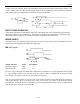
MODE SELECT
The DS1023 has four possible output functions but only two output pins. The functionality of the two
output pins is determined by the Mode Select (MS) pin.
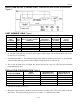
MS = 0 Figure 3
Output Function Name Pin Number
Reference Output REF 9
Delayed Output OUT 15
OUT is a copy of the input waveform that is delayed by an amount set by the programmed values (Table
1). A programmed value of zero will still result in a non-zero delay as indicated in the Step Zero delay
specification. The signal on OUT is the same polarity as the input.
REF is a fixed reference delay. It also is a copy of the input waveform but the delay interval is fixed to a
value approximately equal to the Step Zero Value of the device (as shown in the Reference Delay
specification). In fact the device is trimmed to ensure that the Reference Delay is always slightly longer
than the Step Zero Value (by 1.5 ns typically).