
Datasheet


3.3V Spread-Spectrum EconOscillator
10 Maxim Integrated
DS1086L
The output frequency is determined by the following
equation:
where:
min frequency of selected OFFSET range
is the
lowest frequency (shown in Table 2 for the correspond-
ing offset).
DAC value
is the value of the DAC register (0 to 1023).
Prescaler
is the value of 2
x
where x = 0 to 8.
See the
Example Frequency Calculations
section for a
more in-depth look at using the registers.
________________Register Definitions
The DS1086L registers are used to program the output
frequency, dither percent, dither rate, and 2-wire
address. Table 1 shows a summary of the registers and
detailed descriptions follow below.
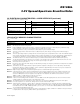
PRESCALER (02h)
The PRESCALER word is a two-byte value containing
control bits for the prescaler (P3 to P0), output control
(Lo/HiZ), the jitter rate (JS4 to JS3), as well as control
bits for the jitter percentage (JS2 to JS0). The
PRESCALER word is read and written using two-byte
reads and writes beginning at address 02h.
JS4 to JS3: Jitter Rate. This is the frequency of the tri-
angle wave generator and the modulation frequency
that the output is dithered. It can be programmed to the
master oscillator frequency, f
OSC
, divided by either
8192, 4096, or 2048.
JS4 JS3 JITTER RATE
00 f
OSC
/8192
01 f
OSC
/4096 (default)
10 f
OSC
/2048
f
OUTPUT
MINFREQUENCY OF SELECTED OFFSET(
=
)
()
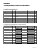
RANGE
DAC VALUE kHz STEP SIZE
PRESC
+×5
AALER
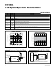
OFFSET FREQUENCY RANGE (MHz)
OS - 6 30.74 to 35.86
OS - 5 33.30 to 38.42
OS - 4 35.86 to 40.98
OS - 3 38.42 to 43.54
OS - 2 40.98 to 46.10
OS - 1 43.54 to 48.66
OS* 46.10 to 51.22
OS + 1 48.66 to 53.78
OS + 2 51.22 to 56.34
OS + 3 53.78 to 58.90
OS + 4 56.34 to 61.46
OS + 5 58.90 to 64.02
OS + 6 61.46 to 66.58
*
Factory default setting. OS is the integer value of the five LSBs
of the RANGE register.
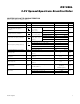
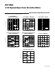
REGISTER ADDR MSB BINARY LSB
FACTORY
DEFAULT
ACCESS
PRESCALER 02h JS4 JS3 JS2 JS1 JS0 LO/HiZ P3 P2 0 1 1 0 0 0 0 0 R/W
PRESCALER — P1 P0 X
X
X
X
X
X
X
X
X
X
X
X
0 0 X X X X X R/W
DAC (MSB) 08h b9 b8 b7 b6 b5 b4 b3 b2 01111101b R/W
DAC (LSB) — b1 b0 X
0
X
0
X
0
X
0
X
0
X
0
00000000b R/W
OFFSET 0Eh X
1
X
1
X
1
b4 b3 b2 b1 b0 1 1 1 - - - - - b R/W
ADDR 0Dh X
1
X
1
X
1
X
1
WC A2 A1 A0 11110000b R/W
RANGE 37h X
X
X
X
X
X
b4 b3 b2 b1 b0 x x x - - - - - b R
WRITE EE 3Fh NO DATA
——
Table 1. Register Summary
X
0
= Don’t care, reads as zero.
X
1
= Don’t care, reads as one.
X
X
= Don’t care, reads indeterminate.
X = Don’t care.
Table 2. Offset Settings