
Datasheet


DS1089L
3.3V Center Spread-Spectrum EconOscillator™
4 _____________________________________________________________________
Note 1: All voltages are referenced to ground.
Note 2: This is the absolute accuracy of the master oscillator frequency at the default settings with spread disabled.
Note 3: This is the change that is observed in master oscillator frequency with changes in voltage at T
A
= +25°C.
Note 4: This is the change that is observed in master oscillator frequency with changes in temperature at V
CC
= 3.3V.
Note 5: The dither deviation of the master oscillator frequency is biderectional and results in an output frequency centered at the
undithered frequency.
Note 6: This indicates the time elapsed between power-up and the output becoming active. An on-chip delay is intentionally intro-
duced to allow the oscillator to stabilize. t
STAB
is equivalent to 512 master clock cycles and will depend on the programmed
master oscillator frequency.
Note 7: Timing shown is for fast-mode (400kHz) operation. This device is also backward compatible with I
2
C standard-mode timing.
Note 8: C
B
—total capacitance of one bus line in picofarads.
Note 9: EEPROM write time applies to all the EEPROM memory and SRAM shadowed EEPROM memory when WC = 0.
The EEPROM write time begins after a stop condition occurs.
Note 10:Typical frequency shift due to aging is ±0.25%. Aging stressing includes Level 1 moisture reflow conditioning (24hr) +125°C
bake, 168hr +85°C/85°RH moisture soak, and three solder reflow passes +260 +0/-5°C peak) followed by 408hr max V
CC
biased 125°C HTOL, 500 temperature cycles at -55°C to +125°C, 96hr +130°C/85%RH/3,6V HAST and 168hr +121°C/2 ATM
Steam/Unbiased Autoclave.
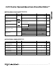
PARAMETER
SYMBOL
CONDITIONS
MIN TYP MAX UNITS
SCL Clock Frequency f
SCL
(Note 7) 0 400 kHz
Bus Free Time Between Stop and
Start Conditions
t
BUF
1.3 µs
Hold Time (Repeated) Start
Condition
t
HD:STA
0.6 µs
Low Period of SCL t
LOW
1.3 µs
High Period of SCL t
HIGH
0.6 µs
Data Hold Time
t
HD:DAT
0 0.9 µs
Data Setup Time
t
SU:DAT
100
ns
Start Setup Time t
SU:STA
0.6 µs
SDA and SCL Rise Time t
R
(Note 8) 20 + 0.1C
B
300 ns
SDA and SCL Fall Time t
F
(Note 8) 20 + 0.1C
B
300 ns
Stop Setup Time
t
SU:STO
0.6 µs
SDA and SCL Capacitive
Loading
C
B
(Note 8) 400 pF
EEPROM Write Time t
WR
(Note 9) 10 20 ms
AC ELECTRICAL CHARACTERISTICS—I
2
C INTERFACE
(V
CC
= +2.7V to +3.6V, T
A
= -40°C to +85°C, unless otherwise noted. Timing referenced to V
IL(MAX)
and V
IH(MIN)
.)
PARAMETER
SYMBOL
CONDITION
MIN TYP MAX
UNITS
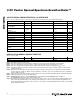
Writes +70°C
10,000
NONVOLATILE MEMORY CHARACTERISTICS
(V
CC
= +2.7V to +3.6V)