
Datasheet


DS1220AB/AD
2 of 8
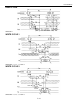
READ MODE
The DS1220AB and DS1220AD execute a read cycle whenever
WE
(Write Enable) is inactive (high) and
CE
(Chip Enable) and
OE
(Output Enable) are active (low). The unique address specified by the 11
address inputs (A0-A10) defines which of the 2048 bytes of data is to be accessed. Valid data will be
available to the eight data output drivers within t
ACC
(Access Time) after the last address input signal is
stable, providing that the
CE
and
OE
access times are also satisfied. If
CE
and
OE
access times are not
satisfied, then data access must be measured from the later-occurring signal and the limiting parameter is
either t
CO
for
CE
or t
OE
for
OE
rather than address access.
WRITE MODE
The DS1220AB and DS1220AD execute a write cycle whenever the
WE
and
CE
signals are active (low)
after address inputs are stable. The latter occurring falling edge of
CE
or
WE
will determine the start of
the write cycle. The write cycle is terminated by the earlier rising edge of
CE
or
WE
. All address inputs
must be kept valid throughout the write cycle.
WE
must return to the high state for a minimum recovery
time (t
WR
) before another cycle can be initiated. The
OE
control signal should be kept inactive (high)
during write cycles to avoid bus contention. However, if the output drivers are enabled (
CE
and
OE
active) then
WE
will disable the outputs in t
ODW
from its falling edge.
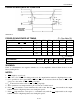
DATA RETENTION MODE
The DS1220AB provides full functional capability for V
CC
greater than 4.75 volts and write protects by
4.5V. The DS1220AD provides full functional capability for V
CC
greater than 4.5 volts and write protects
by 4.25V. Data is maintained in the absence of V
CC
without any additional support circuitry. The
nonvolatile static RAMs constantly monitor V
CC
. Should the supply voltage decay, the NV SRAMs
automatically write protect themselves, all inputs become “don’t care,” and all outputs become high
impedance. As V
CC
falls below approximately 3.0 volts, a power switching circuit connects the lithium
energy source to RAM to retain data. During power-up, when V
CC
rises above approximately 3.0 volts,
the power switching circuit connects external V
CC
to RAM and disconnects the lithium energy source.
Normal RAM operation can resume after V
CC
exceeds 4.75 volts for the DS1220AB and 4.5 volts for the
DS1220AD.
FRESHNESS SEAL
Each DS1220 device is shipped from Dallas Semiconductor with its lithium energy source disconnected,
guaranteeing full energy capacity. When V
CC
is first applied at a level of greater than V
TP
, the lithium
energy source is enabled for battery backup operation.