
Datasheet


NOT RECOMMENDED FOR NEW DESIGNS DS1225Y
7 of 8
8. If
WE
is low or the
WE
low transition occurs prior to or simultaneously with the
CE
low transition,
the output buffers remain in a high-impedance state during this period.
9. Each DS1225Y is marked with a 4-digit date code AABB. AA designates the year of manufacture.
BB designates the week of manufacture. The expected t
DR
is defined as starting at the date of
manufacture.
10. All AC and DC electrical characteristics are valid over the full operating temperature range. For
commercial products, this range is 0°C to 70°C. For industrial products (IND), this range is -40°C to
+85°C.
11. In a power down condition the voltage on any pin may not exceed the voltage on V
CC
.
12. t
WR1
, t
DH1
are measured from
WE
going high.
13. t
WR2
, t
DH2
are measured from
CE
going high.
14. DS1225Y modules are recognized by Underwriters Laboratories (UL) under file E99151 (R).
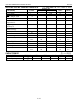
DC TEST CONDITIONS
Outputs open.
All voltages are referenced to ground.
AC TEST CONDITIONS
Output Load: 100pF + 1TTL Gate
Input Pulse Levels: 0-3.0V
Timing Measurement Reference Levels
Input:1.5V Output: 1.5V
Input Pulse Rise and Fall Times: 5ns
ORDERING INFORMATION
PART TEMP RANGE
SUPPLY
TOLERANCE
SPEED GRADE
(ns)
PIN-PACKAGE
DS1225Y-150+
0°C to +70°C
5V ± 10%
150
28 720 EDIP
DS1225Y-
150IND+
-40°C to +85°C
5V ± 10%
150 28 720 EDIP
+Denotes a lead(Pb)-free/RoHS-compliant package.
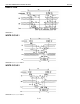
PACKAGE INFORMATION
For the latest package outline information and land patterns, go to www.maxim-ic.com/packages. Note that a “+”,
“#”, or “-” in the package code indicates RoHS status only. Package drawings may show a different suffix
character, but the drawing pertains to the package regardless of RoHS status.
PACKAGE TYPE PACKAGE CODE OUTLINE NO. LAND PATTERN NO.
28 EDIP MDT28+2 21-0245 —