
Datasheet


DS1250Y/AB
2 of 10
DESCRIPTION
The DS1250 4096k Nonvolatile SRAMs are 4,194,304-bit, fully static, nonvolatile SRAMs organized as
524,288 words by 8 bits. Each complete NV SRAM has a self-contained lithium energy source and
control circuitry which constantly monitors V
CC
for an out-of-tolerance condition. When such a condition
occurs, the lithium energy source is automatically switched on and write protection is unconditionally
enabled to prevent data corruption. DIP-package DS1250 devices can be used in place of existing 512k x
8 static RAMs directly conforming to the popular byte-wide 32-pin DIP standard. DS1250 devices in the
PowerCap Module package are directly surface mountable and are normally paired with a DS9034PC
PowerCap to form a complete Nonvolatile SRAM module. There is no limit on the number of write
cycles that can be executed and no additional support circuitry is required for microprocessor interfacing.
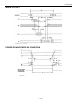
READ MODE
The DS1250 executes a read cycle whenever
WE
(Write Enable) is inactive (high) and
CE
(Chip Enable)
and
OE
(Output Enable) are active (low). The unique address specified by the 19 address inputs (A
0
-
A
18
) defines which of the 524,288 bytes of data is to be accessed. Valid data will be available to the eight
data output drivers within t
ACC
(Access Time) after the last address input signal is stable, providing that
CE
and
OE
(Output Enable) access times are also satisfied. If
OE
and
CE
access times are not satisfied,
then data access must be measured from the later-occurring signal (
CE
or
OE
) and the limiting parameter
is either t
CO
for
CE
or t
OE
for
OE
rather than address access.
WRITE MODE
The DS1250 executes a write cycle whenever the
WE
and
CE
signals are active (low) after address
inputs are stable. The later-occurring falling edge of
CE
or WE will determine the start of the write cycle.
The write cycle is terminated by the earlier rising edge of
CE
or
WE
. All address inputs must be kept
valid throughout the write cycle.
WE
must return to the high state for a minimum recovery time (t
WR
)
before another cycle can be initiated. The
OE
control signal should be kept inactive (high) during write
cycles to avoid bus contention. However, if the output drivers are enabled (
CE
and
OE
active) then
WE
will disable the outputs in t
ODW
from its falling edge.
DATA RETENTION MODE
The DS1250AB provides full functional capability for V
CC
greater than 4.75 volts and write protects by
4.5 volts. The DS1250Y provides full functional capability for V
CC
greater than 4.5 volts and write
protects by 4.25 volts. Data is maintained in the absence of V
CC
without any additional support circuitry.
The nonvolatile static RAMs constantly monitor V
CC
. Should the supply voltage decay, the NV SRAMs
automatically write protect themselves, all inputs become “don’t care,” and all outputs become high-
impedance. As V
CC
falls below approximately 3.0 volts, a power switching circuit connects the lithium
energy source to RAM to retain data. During power-up, when V
CC
rises above approximately 3.0 volts,
the power switching circuit connects external V
CC
to RAM and disconnects the lithium energy source.
Normal RAM operation can resume after V
CC
exceeds 4.75 volts for the DS1250AB and 4.5 volts for the
DS1250Y.
FRESHNESS SEAL
Each DS1250 device is shipped from Maxim with its lithium energy source disconnected, guaranteeing
full energy capacity. When V
CC
is first applied at a level greater than 4.25 volts, the lithium energy source
is enabled for battery back-up operation.