
Datasheet


DS1250Y/AB
8 of 10
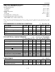
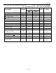
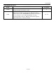
POWER-DOWN/POWER-UP TIMING (T
A
: See Note 10)
PARAMETER SYMBOL MIN TYP MAX UNITS NOTES
V
CC
Fail Detect to
CE
and
WE
Inactive
t
PD
1.5
µs
11
V
CC
slew from V
TP
to 0V t
F
150
µs
V
CC
slew from 0V to V
TP
t
R
150
µs
V
CC
Valid to
CE
and
WE
Inactive
t
PU
2 ms
V
CC
Valid to End of Write Protection t
REC
125 ms
(T
A
= +25°C)
PARAMETER SYMBOL MIN TYP MAX UNITS NOTES
Expected Data Retention Time t
DR
10 years 9
WARNING:
Under no circumstance are negative undershoots, of any amplitude, allowed when device is in battery
backup mode.
NOTES:
1.
WE
is high for a Read Cycle.
2.
OE
= V
IH
or V
IL
. If
OE
= V
IH
during write cycle, the output buffers remain in a high-impedance state.
3. t
WP
is specified as the logical AND of
CE
and
WE
. t
WP
is measured from the latter of
CE
or
WE
going low to the earlier of
CE
or
WE
going high.
4. t
DH
, t
DS
are measured from the earlier of
CE
or
WE
going high.
5. These parameters are sampled with a 5 pF load and are not 100% tested.
6. If the
CE
low transition occurs simultaneously with or latter than the
WE
low transition, the output
buffers remain in a high-impedance state during this period.
7. If the
CE
high transition occurs prior to or simultaneously with the
WE
high transition, the output
buffers remain in high-impedance state during this period.
8. If
WE
is low or the
WE
low transition occurs prior to or simultaneously with the
CE
low transition,
the output buffers remain in a high-impedance state during this period.
9. Each DS1250 has a built-in switch that disconnects the lithium source until the user first applies V
CC
.
The expected t
DR
is defined as accumulative time in the absence of V
CC
starting from the time power
is first applied by the user. This parameter is assured by component selection, process control, and
design. It is not measured directly during production testing.
10. All AC and DC electrical characteristics are valid over the full operating temperature range. For
commercial products, this range is 0°C to 70°C. For industrial products (IND), this range is -40°C to
+85°C.
11. In a power-down condition the voltage on any pin may not exceed the voltage on V
CC
.
12. t
WR1
and t
DH1
are measured from
WE
going high.
13. t
WR2
and t
DH2
are measured from
CE
going high.
14. DS1250 modules are recognized by Underwriters Laboratories (UL) under file E99151.