
Datasheet


DS12885/DS12887/DS12887A/DS12C887/DS12C887A
Real-Time Clocks
2 _____________________________________________________________________
ABSOLUTE MAXIMUM RATINGS
Stresses beyond those listed under “Absolute Maximum Ratings” may cause permanent damage to the device. These are stress ratings only, and functional
operation of the device at these or any other conditions beyond those indicated in the operational sections of the specifications is not implied. Exposure to
absolute maximum rating conditions for extended periods may affect device reliability.
Voltage Range on V
CC
Pin Relative to Ground .....-0.3V to +6.0V
Operating Temperature Range ...................................................
Commercial (noncondensing) .............................0°C to +70°C
Operating Temperature Range ...................................................
Industrial (noncondensing)...............................-40°C to +85°C
Storage Temperature Range
EDIP..................................................................-40°C to +85°C
PDIP, SO, PLCC, TQFP ..................................-55°C to +125°C
Lead Temperature (soldering, 10s) .................................+260°C
(Note: EDIP is hand or wave-soldered only.)
Soldering Temperature (reflow)
PDIP, SO, PLCC............................................................+260°C
TQFP .............................................................................+245°C
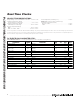
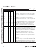
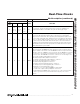
DC ELECTRICAL CHARACTERISTICS
(V
CC
= +4.5V to +5.5V, T
A
= over the operating range, unless otherwise noted.) (Note 2)
PARAMETER SYMBOL CONDITIONS MIN TYP MAX UNITS
Supply Voltage V
CC
(Note 3) 4.5 5.5 V
V
BAT
Input Voltage V
BAT
(Note 3) 2.5 4.0 V
Input Logic 1 V
IH
(Note 3) 2.2
V
CC
+
0.3
V
Input Logic 0 V
IL
(Note 3) -0.3 +0.8 V
V
CC
Power-Supply Current I
CC1
(Note 4) 15 mA
V
CC
Standby Current I
CCS
(Note 5) mA
Input Leakage I
IL
-1.0 +1.0 µA
I/O Leakage I
OL
(Note 6) -1.0 +1.0 µA
Input Current I
MOT
(Note 7) -1.0 +500 µA
Output at 2.4V I
OH
(Note 3) -1.0 mA
Output at 0.4V I
OL
(Note 3) 4.0 mA
Power-Fail Voltage V
PF
(Note 3) 4.0 4.25 4.5 V
VRT Trip Point VRT
TRIP
1.3 V